
LTM4607EV Demo Board | LTM4607(x2) Buck-Boost uModule, 6V ≤ VIN ≤ 36V, VOUT = 12V @ 10A
Analog Devices Inc.Demonstration circuit DC1601B is a PolyPhase® power supply featuring the LTM4607 power module, a complete high efficiency switching mode buck-boost power supply. The DC1601B input voltage range is from 6V to 36V and is capable of delivering high power through paralleled LTM4607 modules. The demo circuit can deliver up to 10A of output current for two paralleled modules (DC1601B-A). The DC1601B demonstrates that paralleling modules is easy and reliable. The output voltage for the board is 12V. The rated load current per module is 5A in boost mode, however current derating may be necessary under certain VIN, VOUT, frequency, and thermal conditions. An onboard external clock is provided for synchronization and interleaving of phases to minimize input and output ripple. An internal phase-locked loop allows the LTM4607 to be synchronized to an external clock within the range of 200kHz to 400kHz. The LTM4607 default switching frequency on the DC1601B is set to 300kHz through the onboard LTC6902 clock generator which interleaves the paralleled phases.

DC1605B
Analog Devices Inc.The LTC2936 is an EEPROM configurable voltage supervisor which can simultaneously monitor up to six power supply voltage inputs. Each voltage detector offers I2C programmable overvoltage/undervoltage thresholds in various ranges and increments and a dedicated comparator output.Two general purpose inputs (GPI) can be configured as programmable manual reset (MR), UV disable (UVDIS), margin (MARG), Write Protect (WP) or auxiliary comparator (AUXC) inputs. Three general purpose pins (GPIO) can be configured for input or output operation. When configured as an input, a GPIO pin can be mapped to any other GPIO configured as output. The GPIO pins can also be configured as ALERT or fault outputs. Faults can be configured with programmable delay-on-release times. Output type and polarity are also configurable.Status and history registers log faults and can be polled via the I2C interface. A fault snapshot is also backed up in internal EEPROM. All parameters are programmable via the I2C interface. Configuration EEPROM supports autonomous operation without additional software.Applications High Availability Computer Systems Network Servers Telecom Equipment Data Storage

LT3745 Demo Board | Three 16-Channel Buck RGB LED Drivers, Requires DC590B, 9V ≤ VIN ≤ 40V, VLED = 3.4V or 4.2V @ 50mA per Channel
Analog Devices Inc.Demonstration circuit 1608A features the LT3745, a 16-channel 50mA buck LED driver controller and serial interface. Each channel drives a single LED. Three LT3745's are connected in series with each one controlling a color in a 16 LED RGD array. Each channel has an individually adjustable 12-bit (4096-step) grayscale PWM dimming control and a 6-bit (64-step) dot correction current adjustment.
The demo board input voltage range is 9V to 40V and the buck controller outputs 3.4V or 4.2V depending on the color of the LED.

LTC2144-14: 14-bit 105Msps Dual ADC, DDR LVDS Outputs, 5-140MHz, Requires DC890, LVDS_XFMR and DC1075
Analog Devices Inc.DC1620A-H: Demo Board for LTC2144-14 14-Bit, 105Msps Low Power Dual ADCs.

LTC2140-14: 14-bit 25Msps Dual ADC, DDR LVDS Outputs, 5-140MHz, Requires DC890, LVDS_XFMR and DC1075
Analog Devices Inc.DC1620A-L: Demo Board for LTC2140-14 14-Bit, 25Msps Low Power Dual ADCs.

DC1625A-D
Analog Devices Inc.The LTC4227 offers ideal diode-OR and Hot Swap? functions for two power rails by controlling external Nchannel MOSFETs. MOSFETs acting as ideal diodes replace two high power Schottky diodes and the associated heat sinks, saving power and board area. A Hot Swap control MOSFET allows a board to be safely inserted and removed from a live backplane by limiting inrush current. The supply output is also protected against short-circuit faults with a fast acting current limit and internal timed circuit breaker.The LTC4227 regulates the forward voltage drop across the MOSFETs to ensure smooth current transfer from one supply to the other without oscillation. The ideal diodes turn on quickly to reduce the load voltage droop during supply switchover. If the input supply fails or is shorted, a fast turn-off minimizes reverse-current transients.The LTC4227 allows turn-on/off control, and reports fault and power good status for the supply. Part Overcurrent Fault Start-Up Delay LTC4227-1 Latch Off 100ms LTC4227-2 Retry 100ms LTC4227-3 Latch Off 1.6ms LTC4227-4 Retry 1.6ms Applications Redundant Power Supplies and Supply Holdup Computer Systems and Servers Telecom Networks

LTC4226CUD-2 Demo Board: Dual Hot Swap Controller with Auto-Retry
Analog Devices Inc.DC1627A-B: Demo Board for the LTC4226 Wide Operating Range Dual Hot Swap Controller.

DC1633B
Analog Devices Inc.The LTC2933 is an EEPROM configurable voltage supervisor which can simultaneously monitor up to six power supply voltage inputs. Each voltage detector offers I2C programmable over/undervoltage thresholds in various ranges and increments.Two general purpose inputs (GPI) can be configured as programmable manual reset (MR), UV disable (UVDIS), margin (MARG) or auxiliary comparator (AUXC) inputs. Three general purpose pins (GPIO) can be configured for input or output operation. When configured as an input, a GPIO pin can be mapped to any other GPIO configured as output. The GPIO pins can also be configured as ALERT or fault outputs. Faults can be configured with programmable delay-on-release times. Output type and polarity are also configurable.Status and history registers log faults and can be polled via the I2C interface. A fault log snapshot is also backed up in internal EEPROM. All parameters are programmable via the I2C interface. Configuration EEPROM supports autonomous operation without additional software.Applications High Availability Computer Systems Network Servers Telecom Equipment Data Storage

DC1635A
Analog Devices Inc.The LTC4412 controls an external P-channel MOSFET to create a near ideal diode function for power switchover or load sharing. This permits highly efficient OR?ing of multiple power sources for extended battery life and low self-heating. When conducting, the voltage drop across the MOSFET is typically 20mV. For applications with a wall adapter or other auxiliary power source, the load is automatically disconnected from the battery when the auxiliary source is connected. Two or more LTC4412s may be interconnected to allow load sharing between multiple batteries or charging of multiple batteries from a single charger.The wide supply operating range supports operation from one to six Li-Ion cells in series. The low quiescent current (11?A typical) is independent of the load current. The gate driver includes an internal voltage clamp for MOSFET protection.The STAT pin can be used to enable an auxiliary P-channel MOSFET power switch when an auxiliary supply is detected. This pin may also be used to indicate to a microcontroller that an auxiliary supply is connected. The control (CTL) input enables the user to force the primary MOSFET off and the STAT pin low.The LTC4412 is available in a low profile (1mm) ThinSOT package. ? Supply Range LTC4412 2.5V ? 28V (36V max) LTC4412HV 2.5V ? 36V (40V max) Applications Cellular Phones Notebook and Handheld Computers Digital Cameras USB-Powered Peripherals Uninterruptible Power Supplies Logic Controlled Power Switch

DC1646A
Analog Devices Inc.The LTC5564 is a precision, RF power detector for applications in the 600MHz to 15GHz frequency range. The LTC5564 operates with input power levels from ?24dBm to 16dBm.A temperature compensated Schottky diode peak detector, gain-selectable operational amplifier, and fast comparator are combined in a small 16-lead 3mm ? 3mm QFN package.The RF input signal is peak detected and then sensed by both a comparator and amplifier. The comparator provides a 9ns response time to input levels exceeding VREF along with a latch enable/disable function. The gain selectable operational amplifier provides a 350V/?s slew rate and 75MHz of demodulation bandwidth to the analog output.VOUTADJ and VREF pins allow for the adjustment of VOUT offset and VCOMP switch point voltages, respectively.Applications RF Signal Presence Detectors for: 802.11a, 802.11b,?802.11g, 802.15, Optical Data Links, Wireless Data?Modems, Wireless and Cable Infrastructure 5.8GHz ISM Band Radios MMDS Microwave Links PA Power Supply Envelope Tracking Control Fast Alarm RF Power Monitor Envelope Detector Ultra-Wideband Radio Radar Detector

LTC6803-2 (Requires DC590B) | Demo Board
Analog Devices Inc.DC1652A: Demo Board for LTC6803-2 and -4 Multicell Battery Stack Monitor.

LTC3388EMSE-1 Demo Board | 2.7V ≤ VIN ≤ 20V, VOUT = 1.2V to 2.5V @ 50mA
Analog Devices Inc.Demonstration Circuit DC1658A is a 20V High Efficiency Nanopower Step-Down Regulator featuring the LTC3388-1/ LTC3388-3. The LTC3388 is an ultralow quiescent current power supply designed to regulate the output voltage by means of a nanopower high efficiency synchronous buck regulator. The input current is only 720nA typical at no load while maintaining output voltage regulation, capable of supplying 50mA of load current. The LTC3388-1/ LTC3388-3 also incorporates an accurate undervoltage lockout feature to disable the converter and maintain a low quiescent current state when the input voltage falls below 2.3V. In regulation, the LTC3388-1/LTC3388-3 enter a sleep state in which both input and output quiescent currents are minimal. The buck converter turns on and off as needed to maintain regulation. An additional standby mode disables the buck switching while the output is in regulation for short duration loads requiring low ripple.

LT6109-1 | High Side Current Sense with Reference and Comparators
Analog Devices Inc.DC1659A-A: Demo Board for the LT6109 High Side Current Sense Amplifier with Reference and Comparators.

LTC3109EUF Demo Board | Auto-polarity, Ultralow Voltage Step-Up Converter and Power Manager
Analog Devices Inc.DC1664A: Demo Board for the LTC3109 Auto-Polarity, Ultralow Voltage Step-Up Converter and Power Manager.

DC1668B-C
Analog Devices Inc.The LTM4627 is a complete 15A output high efficiency switch mode DC/DC power supply. Included in the package are the switching controller, power FETs, inductor and compensation components. Operating over an input voltage range from 4.5V to 20V, the LTM4627 supports an output voltage range of 0.6V to 5V, set by a single external resistor. Only a few input and output capacitors are needed.Current mode operation allows precision current sharing of up to four LTM4627 regulators to obtain 60A output. High switching frequency and a current mode architecture enable a very fast transient response to line and load changes without sacrificing stability. The device supports frequency synchronization, multiphase/current sharing operation, Burst Mode operation and output voltage tracking for supply rail sequencing.The LTM4627 is offered in thermally enhanced 15mm ? 15mm ? 4.32mm LGA and 15mm ? 15mm ? 4.92mm BGA packages. The LTM4627 is available with SnPb (BGA) or RoHS compliant terminal finish.Applications Telecom Servers and Networking Equipment ATCA and Storage Cards Industrial Equipment Medical Systems
DC1674A-B
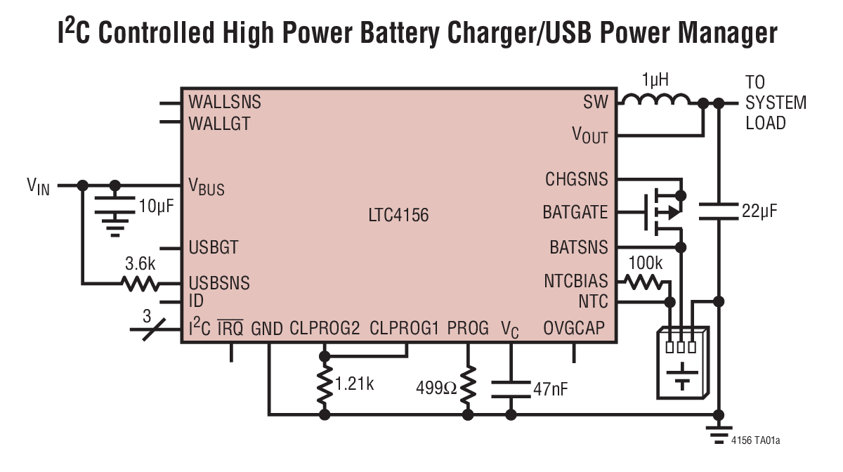
Analog Devices Inc.The LTC4156 is a 15 watt I2C controlled power manager with PowerPath? instant-on operation, high efficiency switching battery charging and USB compatibility. The LTC4156 seamlessly manages power distribution from two 5V sources, such as a USB port and a wall adapter, to a single-cell rechargeable lithium iron phosphate battery and a system load.The LTC4156?s switching battery charger automatically limits its input current for USB compatibility, or may draw up to 3A from a high power wall adapter. The high efficiency step-down switching charger is designed to provide maximum power to the application and reduced heat in high power density applications.I2C adjustability of input current, charge current, battery float voltage, charge termination, and many other parameters allows maximum flexibility. I2C status reporting of key system and charge parameters facilitates intelligent control decisions. USB On-The-Go support provides 5V power back to the USB port without any additional components. A dual-input, priority multiplexing, overvoltage protection circuit guards the LTC4156 from high voltage damage on the VBUS pin.The LTC4156 is available in the low profile (0.75mm) 28-lead 4mm ? 5mm QFN surface mount package.Applications Portable Medical Devices Portable Industrial Devices Backup Devices

LTC2654-H16 Demo Board | Quad SPI 16-Bit Voltage Output DAC with 2.048V Reference, Requires DC2026
Analog Devices Inc.Demonstration circuit 1678A features the LTC2654 Quad 16-bit/12-bit DAC. The LTC2654 is a family of 16-bit/12-bit rail-to-rail DACs with integrated 10ppm/°C maximum reference. The LTC2654 advances performance standards for output drive, crosstalk and load regulation in single supply, voltage-output multiple DACs.
LTC2654-L12 Quad SPI 12-Bit Voltage Output DAC with 1.25V Reference, Requires DC2026
Analog Devices Inc.Demonstration circuit 1678A features the LTC2654 Quad 16-bit/12-bit DAC. The LTC2654 is a family of 16-bit/12-bit rail-to-rail DACs with integrated 10ppm/°C maximum reference. The LTC2654 advances performance standards for output drive, crosstalk and load regulation in single supply, voltage-output multiple DACs.
DC1678A-D
Analog Devices Inc.The LTC2654 is a family of quad 16-/12-bit rail-to-rail DACs with integrated 10ppm/?C maximum reference . The DACs have built-in high performance, rail-to-rail, output buffers and are guaranteed monotonic. The LTC2654-L has a full-scale output of 2.5V with the integrated reference and operates from a single 2.7V to 5.5V supply. The LTC2654-H has a full-scale output of 4.096V with the integrated reference and operates from a 4.5V to 5.5V supply. Each DAC can also operate with an external reference, which sets the full-scale output to 2 times the external reference voltage. These DACs communicate via a SPI/MICROWIRE? compatible 4-wire serial interface which operates at clock rates up to 50MHz. The LTC2654 incorporates a power-on reset circuit that is controlled by the PORSEL pin. If PORSEL is tied to GND the DACs reset to zero-scale. If PORSEL is tied to VCC, the DACs reset to mid-scale.Applications Mobile Communications Process Control and Industrial Automation Instrumentation Automatic Test Equipment Automotive

LT3652HVEDD Demo Board | 17.7V to 34VIN, Buck 12V Lead Acid@2A, MPPC for Solar Power Input
Analog Devices Inc.Demonstration circuit 1688A is a sealed-lead acid 2A battery charger for solar power applications featuring the LT3652HVEDD. The LT3652HV is a complete mid-power battery charger that can operate over a wide input voltage range. The charger employs a 3.3V battery voltage feedback reference that allows the voltage for charging to be adjusted up to 18V. The LT3652HV has an input voltage regulation loop which reduces charge current if the input falls below a programmed level, set with a resistor divider.
The circuit provides constant-current/constant-voltage charging with a maximum charge current of 2A that is programmed by a current sense resistor.


