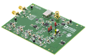
ADL5531-EVALZ
Analog Devices Inc.The ADL5531 is a broadband, fixed-gain, linear amplifier that operates at frequencies up to 500 MHz. The device can be used in a wide variety of equipment, including cellular, satellite, broadband, and instrumentation equipment.The ADL5531 provides a gain of 20 dB, which is stable over frequency, temperature, power supply, and from device to device. This amplifier is single-ended and internally matched to 50 ?. Only input/output ac coupling capacitors, power supply decoupling capacitors, and external inductors are required for operation.The ADL5531 is fabricated on a GaAs HBT process and has an ESD rating of ?2 kV (Class 2). The device is packaged in an 8-lead 3 mm ? 3 mm LFCSP that uses an exposed paddle for excellent thermal impedance.The ADL5531 consumes 100 mA on a single 5 V supply and is fully specified for operation from ?40?C to +85?C.The dual-channel 20 dB gain version, ADL5534, is also available.

ADL5569-EVALZ
Analog Devices Inc.The ADL5569 is a high performance, dual, differential amplifier with 20 dB of voltage gain, optimized for applications spanning from dc to 6.5 GHz. The amplifier is available in a dual format, and it offers a low referred to input (RTI) noise spectral density (NSD) of 1.0 nV/?Hz (at 100 MHz) and excellent distortion performance over a wide frequency range, making it an ideal driver for high speed 12-bit to 16-bit analog-to-digital converters (ADCs). The ADL5569 is ideally suited for use in high performance zero intermediate frequency (IF) and complex IF receiver designs. In addition, this device has excellent low distortion for single-ended input driver applications.Using two external series resistors for each amplifier expands the gain flexibility of the amplifier and allows any gain selection from 6 dB to 20 dB for a differential input. For a single-ended input, the gain can be adjusted from 6 dB to 17 dB with the addition of some external resistors. This device maintains low distortion through its output common-mode range of 2.0 V to 3.0 V, providing a flexible capability for driving ADCs with ac levels up to 2 VP-P.Operating from a single 5 V supply, the quiescent current of the ADL5569 is typically 86 mA per amplifier. When disabled, the amplifiers consume only 8 mA per amplifier.The device is optimized for wideband, low distortion, and low noise operation, giving it unprecedented second harmonic distortion (HD2) and third harmonic distortion (HD3) from dc to 4 GHz. These attributes, together with its adjustable gain capability, make this device the amplifier of choice for driving a wide variety of ADCs, mixers, pin diode attenuators, surface acoustic wave (SAW) filters, and a multitude of discrete radio frequency (RF) devices.Fabricated on an Analog Devices, Inc., high speed silicon germanium (SiGe) process, the ADL5569 is supplied in a compact 2.5 mm ? 3 mm, 16-lead LFCSP package and operates over the ?40?C to +85?C temperature range.APPLICATIONS Differential ADC drivers for GSPS ADCs High speed data acquisition Single-ended to differential conversion DAC buffering DC coupling and level shifting RF/IF gain blocks Balun alternative from dc to 4 GHz SAW filter interfacing

ADP2138CB-1.0EVALZ
Analog Devices Inc.The ADP2138 and ADP2139 are high efficiency, low quiescent current, synchronous step-down dc-to-dc converters. The ADP2139 has the additional feature of an internal discharge switch. The total solution requires only three tiny external components. When the MODE pin is set high, the buck regulator operates in forced PWM mode, which provides low peak-to-peak ripple for power supply noise sensitive loads at the expense of light load efficiency. When the MODE pin is set low, the buck regulator automatically switches operating modes, depending on the load current level. At higher output loads, the buck regulator operates in PWM mode. When the load current falls below a predefined threshold, the regulator operates in power save mode (PSM), improving light load efficiency.The ADP2138/ADP2139 operate on input voltages of 2.3 V to 5.5 V, which allows for single lithium or lithium polymer cell, multiple alkaline or NiMH cell, PCMCIA, USB, and other standard power sources. The maximum load current of 800 mA is achievable across the input voltage range.The ADP2138/ADP2139 are available in fixed output voltages of 3.3 V, 3.0 V, 2.8 V, 2.5 V, 1.8 V, 1.5 V, 1.2 V, 1.0 V, and 0.8 V. All versions include an internal power switch and synchronous rectifier for minimal external part count and high efficiency. The ADP2138/ADP2139 have internal soft start and they are internally compensated. During logic controlled shutdown, the input is disconnected from the output and the ADP2138/ADP2139 draw 0.2 ?A (typical) from the input source.Other key features include undervoltage lockout to prevent deep battery discharge, and soft start to prevent input current overshoot at startup. The ADP2138/ADP2139 are available in a 6-ball wafer level chip scale package (WLCSP).Applications PDAs and palmtop computers Wireless handsets Digital audio, portable media players Digital cameras, GPS navigation units
ADP2138CB-3.0EVALZ
Analog Devices Inc.The ADP2138 and ADP2139 are high efficiency, low quiescent current, synchronous step-down dc-to-dc converters. The ADP2139 has the additional feature of an internal discharge switch. The total solution requires only three tiny external components. When the MODE pin is set high, the buck regulator operates in forced PWM mode, which provides low peak-to-peak ripple for power supply noise sensitive loads at the expense of light load efficiency. When the MODE pin is set low, the buck regulator automatically switches operating modes, depending on the load current level. At higher output loads, the buck regulator operates in PWM mode. When the load current falls below a predefined threshold, the regulator operates in power save mode (PSM), improving light load efficiency.The ADP2138/ADP2139 operate on input voltages of 2.3 V to 5.5 V, which allows for single lithium or lithium polymer cell, multiple alkaline or NiMH cell, PCMCIA, USB, and other standard power sources. The maximum load current of 800 mA is achievable across the input voltage range.The ADP2138/ADP2139 are available in fixed output voltages of 3.3 V, 3.0 V, 2.8 V, 2.5 V, 1.8 V, 1.5 V, 1.2 V, 1.0 V, and 0.8 V. All versions include an internal power switch and synchronous rectifier for minimal external part count and high efficiency. The ADP2138/ADP2139 have internal soft start and they are internally compensated. During logic controlled shutdown, the input is disconnected from the output and the ADP2138/ADP2139 draw 0.2 ?A (typical) from the input source.Other key features include undervoltage lockout to prevent deep battery discharge, and soft start to prevent input current overshoot at startup. The ADP2138/ADP2139 are available in a 6-ball wafer level chip scale package (WLCSP).Applications PDAs and palmtop computers Wireless handsets Digital audio, portable media players Digital cameras, GPS navigation units

ADP2140CPZ-REDYKIT
Analog Devices Inc.The ADP2140 includes a high efficiency, low quiescent 600 mAstepdown dc-to-dc converter and a 300 mA LDO packaged in asmall 10-lead 3 mm ? 3 mm LFCSP. The total solution requiresonly four tiny external components.The buck regulator uses a proprietary high speed current-mode,constant frequency, pulse-width modulation (PWM) controlscheme for excellent stability and transient response. To ensurethe longest battery life in portable applications, the ADP2140 hasa power saving variable frequency mode to reduce switching frequencyunder light loads.The LDO is a low quiescent current, low dropout linear regulatordesigned to operate in a split supply mode with VIN2 as low as1.65 V. The low input voltage minimum allows the LDO to bepowered from the output of the buck regulator increasing efficiencyand reducing power dissipation. The ADP2140 runs frominput voltages of 2.3 V to 5.5 V allowing single Li+/Li? polymer cell, multiple alkaline/NiMH cell, PCMCIA, and other standardpower sources.ADP2140 includes a power-good pin, soft start, and internal?compensation. Numerous power sequencing options are user-selectable through two enable inputs. In autosequencing mode, the highest voltage output enables on the rising edge of EN1.?During logic controlled shutdown, the input disconnects from the output and draws less than 300 nA from the input source.?Other key features include: undervoltage lockout to prevent deep?battery discharge, soft start to prevent input current overshoot?at startup, and both short-circuit protection and thermal overload protection circuits to prevent damage in adverse conditions.When the ADP2140 is used with two 0603 capacitors, one 0402capacitor, one 0402 resistor, and one 0805 chip inductor, the totalsolution size is approximately 90 mm2 resulting in the smallest footprintsolution to meet a variety of portable applications.Applications Mobile phones Personal media players Digital camera and audio devices Portable and battery-powered equipment

ADP2380-EVALZ
Analog Devices Inc.The ADP2380 is a current mode control, synchronous, step-down, dc-to-dc regulator. It integrates a 44 m? high-side power MOSFET and a low-side driver to provide a high efficiency solution. The ADP2380 runs from an input voltage of 4.5 V to 20 V and can deliver 4 A of output current. The output voltage can be adjusted to 0.6 V to 90% of the input voltage. The switching frequency of the ADP2380 can be programmed from 250 kHz to 1.4 MHz or fixed at 290 kHz or 540 kHz. The synchronization function allows the switching frequency to be synchronized to an external clock to minimize system noise.External compensation and an adjustable soft start provide design flexibility. The power-good output provides simple and reliable power sequencing. Additional features include programmable undervoltage lockout (UVLO), overvoltage protection (OVP), overcurrent protection (OCP), and thermal shutdown (TSD).The ADP2380 operates over the ?40?C to +125?C junction temperature range and is available in a 16-lead TSSOP_EP package.APPLICATIONS Communication infrastructure Networking and servers Industrial and instrumentation Healthcare and medical Intermediate power rail conversion DC-to-dc point of load application

ADP2441-EVALZ
Analog Devices Inc.The?ADP2441/ADP2442 is a constant frequency, current mode control, synchronous, step-down dc-to-dc regulator that is capable of driving loads up to 1 A with excellent line and load regulation characteristics. The ADP2441 operates with a wide input voltage range of 4.5 V to 36 V, which makes it ideal for regulating power from a wide variety of sources. In addition, the ADP2441 has very low minimum on time (50 ns) and is, therefore, suitable for applications requiring a very high step-down ratio.The output voltage can be adjusted from 0.6 V to 0.9 V ? VIN. High efficiency is obtained with integrated low resistance N-channel MOSFETs for both high-side and low-side devices.The switching frequency is adjustable from 300 kHz to 1 MHz with an external resistor. The ADP2441 also has an accurate power-good (PGOOD) open-drain output signal.At light load conditions, the regulator operates in pulse skip mode by skipping pulses and reducing switching losses to improve energy efficiency. In addition, at medium to heavy load conditions, the regulator operates in fixed frequency pulse-width modulation (PWM) mode to reduce electromagnetic interference (EMI).The ADP2441 uses hiccup mode to protect the IC from short circuits or from overcurrent conditions on the output. The external programmable soft start limits inrush current during startup for a wide variety of load capacitances. Other key features include tracking, input undervoltage lockout (UVLO), thermal shutdown (TSD), and precision enable (EN), which can also be used as a logic level shutdown input.The ADP2441 is available in a 3 mm ? 3 mm, 12-lead LFCSP package and is rated for a junction temperature range of ?40?C to +125?C.Applications Point of load applications Distributed power systems Industrial control supplies Standard rail conversion to 24 V/12 V/5 V/3.3 V

ADP5023CP-EVALZ
Analog Devices Inc.The ADP5023 combines two high performance buck regulators and one low dropout (LDO) regulator in a small, 24-lead 4 mm ? 4 mm LFCSP to meet demanding performance and board space requirements.The high switching frequency of the buck regulators enables tiny multilayer external components and minimizes the board space. When the MODE pin is set high, the buck regulators operate in forced PWM mode. When the MODE pin is set low, the buck regulators operate in PWM mode when the load current is?above a predefined threshold. When the load current falls below a predefined threshold, the regulator operates in power save mode (PSM) improving the light-load efficiency.The two bucks operate out of phase to reduce the input capacitor requirement. The low quiescent current, low dropout voltage, and wide input voltage range of the ADP5023 LDO extends the battery life of portable devices. The ADP5023 LDO maintains power supply rejection greater than 60 dB for frequencies as high as 10 kHz while operating with a low headroom voltage.Regulators in the ADP5023 are activated though dedicated enable pins. The default output voltages can be externally set in the adjustable version or factory programmable to a wide range of preset values in the fixed voltage version.Applications Power for processors, ASIC, FPGAs, and RF chipsets Portable instrumentation and medical devices Space constrained devices
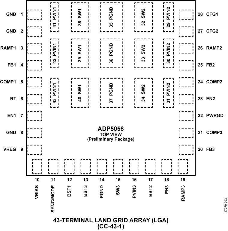
ADP5056-EVALZ
Analog Devices Inc.The ADP5056 combines three high performance buck regulatorsin a 43-terminal land grid array (LGA) package that meets thedemanding performance and board space requirements. Thedevice enables direct connection to high input voltages up to18 V with no preregulators.All channels integrate both high-side and low-side power metaloxide semiconductor field effect transistors (MOSFETs) to achievean efficiency optimized solution. Channel 1 and Channel 2deliver a programmable output current of 3.5 A or 7 A, orprovide a single output with up to 14 A of current in paralleloperation. Channel 3 delivers a programmable output currentof 1.5 A or 3 A.The switching frequency of the ADP5056 can be programmedor synchronized to an external clock. The ADP5056 contains anenable pin (ENx) on each channel for easy power-up sequencingor adjustable undervoltage lockout (UVLO) threshold.The ADP5056 integrates start-up/shutdown sequence control,forced pulse-width modulation/power saving mode (FPWM/PSM)selection, an output discharge switch, and a power-good signal.The ADP5056 is rated at ?40?C to +150?C junction temperature.Note that throughout this data sheet, multifunction pins, suchas SYNC/MODE, are referred to either by the entire pin nameor by a single function of the pin, for example, SYNC, whenonly that function is relevant. Small cell base stations Field programmable gate array (FPGA) and processorapplications Security and surveillance Medical applications

ADP5061CB-EVALZ
Analog Devices Inc.The ADP5061 charger is fully compliant with USB 3.0 and the USB Battery Charging Specification 1.2 and enables charging via the mini USB VBUS pin from a wall charger, car charger, or USB host port.The ADP5061 operates from a 4 V to 6.7 V input voltage range but is tolerant of voltages up to 20 V. The 20 V voltage tolerance alleviates the concerns about the USB bus spiking during disconnect or connect scenarios.The ADP5061 features an internal FET between the linear charger output and the battery. This permits battery isolation and, hence, system powering under a dead battery or no batteryscenario, which allows for immediate system function on connection to a USB power supply.Based on the type of USB source, which is detected by an external USB detection chip, the ADP5061 can be set to apply the correct current limit for optimal charging and USB compliance.The ADP5061 has three factory programmable digital input/output pins that provide maximum flexibility for different systems. These digital input/output pins permit combinations of features such as, input current limits, charging enable and disable, charging current limits, and a dedicated interrupt output pin. APPLICATIONS Digital still cameras Digital video cameras Single cell Li-Ion portable equipment PDAs, audio, GPS devices Portable medical devices Mobile phones

ADP5070CP-EVALZ
Analog Devices Inc.The ADP5070 is a dual high performance dc-to-dc regulator that generates independently regulated positive and negative rails.The input voltage range of 2.85 V to 15 V supports a wide variety of applications. The integrated main switch in both regulators enables generation of an adjustable positive output voltage up to +39 V and a negative output voltage down to ?39 V below input voltage.The ADP5070 operates at a pin selected 1.2 MHz/2.4 MHz switching frequency. The ADP5070 can synchronize with an external oscillator from 1.0 MHz to 2.6 MHz to ease noise filtering in sensitive applications. Both regulators implement programmable slew rate control circuitry for the MOSFET driver stage to reduce electromagnetic interference (EMI).Flexible start-up sequencing is provided with the options of manual enable, simultaneous mode, positive supply first, and negative supply first.The ADP5070 includes a fixed internal or resistor programmable soft start timer to prevent inrush current at power-up. During shutdown, both regulators completely disconnect the loads from the input supply to provide a true shutdown.Other key safety features in the ADP5070 include overcurrent protection (OCP), overvoltage protection (OVP), thermal shutdown (TSD), and input undervoltage lockout (UVLO).The ADP5070 is available in a 20-lead LFCSP or in a 20-lead TSSOP and is rated for a ?40?C to +125?C junction temperature range.Applications Bipolar amplifiers, ADCs, DACs and multiplexers Charge-coupled device (CCD) bias supply Optical module supply RF power amplifier (PA) bias

ADP5075CB-EVALZ
Analog Devices Inc.The ADP5075 is a high performance dc-to-dc inverting regulator used to generate negative supply rails.The input voltage range of 2.85 V to 15 V supports a wide variety of applications. The integrated main switch enables the generation of an adjustable negative output voltage down to 39 V below the input voltage.The ADP5075 operates at a pin selected 1.2 MHz/2.4 MHz switching frequency. The ADP5075 can synchronize with an external oscillator from 1.0 MHz to 2.6 MHz to ease noise filtering in sensitive applications. The regulator implements programmable slew rate control circuitry for the MOSFET driver stage to reduce electromagnetic interference (EMI).The ADP5075 includes a fixed internal or resistor programmable soft start timer to prevent inrush current at power-up. During shutdown, the regulator completely disconnects the load from the input supply to provide a true shutdown.Other key safety features in the ADP5075 include overcurrent protection (OCP), overvoltage protection (OVP), thermal shutdown (TSD), and input undervoltage lockout (UVLO).The ADP5075 is available in a 12-ball WLCSP and is rated for a ?40?C to +125?C junction temperature range.Applications Bipolar amplifiers, analog-to-digital converters (ADCs), ?digital-to-analog converters (DACs), and multiplexers Charge coupled device (CCD) bias supplies Optical module supplies Radio Frequency (RF) power amplifier (PA) bias

ADP5091-2-EVALZ
Analog Devices Inc.The ADP5091/ADP5092 are intelligent, integrated energy harvesting, ultralow power management unit (PMU) solutions that convert dc power from PV cells or TEGs. These devices charge storage elements such as rechargeable Li-Ion batteries, thin film batteries, super capacitors, or conventional capacitors, and power up small electronic devices and battery free systems.The ADP5091/ADP5092 provide efficient conversion of the harvested limited power from a 6 ?W to 600 mW range with submicrowatt operation losses. With the internal cold start circuit, the regulator can start operating at an input voltage as low as 380 mV. After cold startup, the regulator is functional at an input voltage range of 0.08 V to 3.3 V. An additional 150 mA regulated output can be programmed by an external resistor divider or the VID pin.The MPPT control keeps the input voltage ripple in a fixed range to maintain stable dc-to-dc boost conversion. The dynamic sensing mode and no sensing mode, both programming regulation points of the input voltage, allow extraction of the highest possible energy from the harvester. A programmable minimum operation threshold enables boost shutdown during a low input condition.As a low light indicator for a microprocessor, the LLD pin of the ADP5091 is the MINOP comparator output. However, the REG_GOOD flag of the ADP5092 monitors the REG_OUT voltage. In addition, the DIS_SW pin can temporarily shut down the boost regulator and is RF transmission friendly.The charging control function of the ADP5091/ADP5092 protects the rechargeable energy storage, which is achieved by monitoring the battery voltage with the programmable charging termination voltage and the shutdown discharging voltage. In addition, a programmable PGOOD flag monitors the SYS voltage.An optional primary cell battery can be connected and managed by an integrated power path management control block that is programmable to switch the power source from the energy harvester, rechargeable battery, and primary cell battery.The ADP5091/ADP5092 are available in a 24-lead LFCSP and are rated for a ?40?C to +125?C temperature range.Applications Photovoltaic (PV) cell energy harvesting Thermoelectric generators (TEGs) energy harvesting Industrial monitoring Self powered wireless sensor devices Portable and wearable devices with energy harvesting

ADP5135CP-EVALZ
Analog Devices Inc.The ADP5135 combines three high performance buck regulators. It is available in a 24-lead 4 mm ? 4 mm LFCSP.The high switching frequency of the buck regulators enables tiny multilayer external components and minimizes the board space. When the MODE pin is set to high, the buck regulators operate in forced PWM mode. When the MODE pin is set to low, the buck regulators operate in PWM mode only when the load is above a predefined threshold. When the load current falls below this predefined threshold, the regulator operates in power save mode (PSM), improving the light load efficiency.Buck1 and Buck2 operate in sync and Buck3 operates out of phase to reduce the input capacitor requirement. Regulators in the ADP5135 are activated through dedicated enable pins. The default output voltages can be externally set in the adjustable version, or factory programmable to a wide range of preset values in the fixed voltage version.Applications Power for processors, ASICS, FPGAs, and RF chipsets Portable instrumentation and medical devices Space constrained devices

ADP5310READJ-EVALZ
Analog Devices Inc.The ADP5310 combines dual buck regulators and one load switchin a 16-lead TSSOP_EP package that meets demanding performanceand board space requirements. The device enables directconnection to a wide input voltage range of 2.7 V to 15.0 V, allowingthe use of multiple alkaline/NiMH or lithium cells and otherpower sources.The buck regulator in Channel 1 uses a current mode, constantfrequency pulse-width modulation (PWM) control scheme forexcellent stability and transient performance, which provides upto 800 mA of output current. The automatic PWM/pulse skippingmode (PSM) control scheme achieves excellent efficiency in lightoutput current. A power-good signal indicates that the outputof Channel 1 is within 92% of its nominal value.An ultralow power buck regulator is integrated in Channel 2 withthe SYNC/MODE pin to control its operation mode. WhenSYNC/MODE is set to low, the buck regulator operates in hysteresismode, which draws only 700 nA of quiescent current to regulatethe output under zero load and provides up to 50 mA of outputcurrent. Hysteresis mode helps achieve excellent efficiency at lessthan 1 mW and can work as a keep-alive power supply in a batterypoweredsystem. When the SYNC/MODE pin is set to high, thebuck regulator switches to a traditional constant frequency PWMcontrol scheme to provide low output ripple for noise sensitiveapplications, and the buck regulator provides up to 300 mA ofoutput current in PWM mode.Channel 3 integrates a high-side load switch that operates from1.65 V to 5.5 V with its input connected to the output of Channel 2.The load switch provides power domain isolation and extendsbattery operation time.Other key safety features of the ADP5310 include overcurrentprotection (OCP), thermal shutdown (TSD), and input undervoltagelockout (UVLO). The ADP5310 is rated for the ?40?Cto +125?C junction temperature range.Applications Energy (gas and water) metering Portable and battery-powered equipment Medical applications? Keep-alive power supplies

ADP7104RD-EVALZ
Analog Devices Inc.The ADP7104 is a CMOS, low dropout linear regulator that operates from 3.3 V to 20 V and provides up to 500 mA of output current. This high input voltage LDO is ideal for regulation of high performance analog and mixed signal circuits operating from 19 V to 1.22 V rails. Using an advanced proprietary architecture, it provides high power supply rejection, low noise, and achieves excellent line and load transient response with just a small 1 ?F ceramic output capacitor.The ADP7104 is available in seven fixed output voltage options and an adjustable version, which allows output voltages that range from 1.22 V to VIN ? VDO via an external feedback divider.The ADP7104 output noise voltage is 15 ?V rms and is independent of the output voltage. A digital power-good output allows power system monitors to check the health of the output voltage. A user programmable precision undervoltage lockout function facilitates sequencing of multiple power supplies. The ADP7104 is available in 8-lead, 3 mm ? 3 mm LFCSP and 8-lead SOIC packages. The LFCSP offers a very compact solution and also provides excellent thermal performance for applications requiring up to 500 mA of output current in a small, low-profile footprint. APPLICATIONS Regulation to noise sensitive applications:?ADC, DAC circuits, precision amplifiers, high frequency oscillators, clocks, and PLLs Communications and infrastructure Medical and healthcare Industrial and instrumentation
ADP7104RDZ-REDYKIT
Analog Devices Inc.The ADP7104 is a CMOS, low dropout linear regulator that operates from 3.3 V to 20 V and provides up to 500 mA of output current. This high input voltage LDO is ideal for regulation of high performance analog and mixed signal circuits operating from 19 V to 1.22 V rails. Using an advanced proprietary architecture, it provides high power supply rejection, low noise, and achieves excellent line and load transient response with just a small 1 ?F ceramic output capacitor.The ADP7104 is available in seven fixed output voltage options and an adjustable version, which allows output voltages that range from 1.22 V to VIN ? VDO via an external feedback divider.The ADP7104 output noise voltage is 15 ?V rms and is independent of the output voltage. A digital power-good output allows power system monitors to check the health of the output voltage. A user programmable precision undervoltage lockout function facilitates sequencing of multiple power supplies. The ADP7104 is available in 8-lead, 3 mm ? 3 mm LFCSP and 8-lead SOIC packages. The LFCSP offers a very compact solution and also provides excellent thermal performance for applications requiring up to 500 mA of output current in a small, low-profile footprint. APPLICATIONS Regulation to noise sensitive applications:?ADC, DAC circuits, precision amplifiers, high frequency oscillators, clocks, and PLLs Communications and infrastructure Medical and healthcare Industrial and instrumentation

ADP7112CB-EVALZ
Analog Devices Inc.The ADP7112 is a CMOS, low dropout (LDO) linear regulator that operates from 2.7 V to 20 V and provides up to 200 mA of output current. This high input voltage LDO is ideal for the regulation of high performance analog and mixed signal circuits operating from 20 V down to 1.2 V rails. Using an advanced proprietary architecture, the device provides high power supply rejection, low noise, and achieves excellent line and load transient response with a small 2.2 ?F ceramic output capacitor. The ADP7112?regulator output noise is 11 ?V rms independent of the output voltage for the fixed options of 5 V or less.The ADP7112?is available in 16 fixed output voltage options. The following voltages are available from stock: 1.2 V (adjustable), 1.8 V, 2.5 V, 3.3 V, and 5.0 V. Additional voltages available by special order are 1.5 V, 1.85 V, 2.0 V, 2.2 V, 2.75 V, 2.8 V, 2.85 V, 3.8 V, 4.2 V, and 4.6 V.Each fixed output voltage can be adjusted above the initial set point with an external feedback divider. This allows the ADP7112?to provide an output voltage from 1.2 V to VIN ? VDO with high PSRR and low noise.User programmable soft start with an external capacitor is available in the?ADP7112. The ADP7112?is available in a 6-ball 1 mm ? 1.2mm WLCSP, making it a very compact solution.Applications Regulation to noise sensitive applications ADC, DAC circuits, precision amplifiers, power for VCO VTUNE control Communications and infrastructure Medical and healthcare Industrial and instrumentation

ADP7157CP-04-EVALZ
Analog Devices Inc.The ADP7157 is an adjustable linear regulator that operates from 2.3 V to 5.5 V and provides up to 1.2 A of output current. Output voltages from 1.2 V to 3.3 V are possible depending on the model. Using an advanced proprietary architecture, the device provides high power supply rejection and ultralow noise, achieving excellent line and load transient response with only a 10 ?F ceramicoutput capacitor.The ADP7157 is available in four models that optimize powerdissipation and PSRR performance as a function of the inputand output voltage.The typical output noise the ADP7157 regulator is 0.9 ?V rms from 100 Hz to 100 kHz and 1.7 nV/?Hz for noise spectral density from 10 kHz to 1 MHz. The ADP7157 is available in 10-lead, 3 mm ?3 mm LFCSP and 8-lead SOIC packages, making it not only avery compact solution, but also providing excellent thermalperformance for applications requiring up to 1.2 A of outputcurrent in a small, low profile footprint.Applications Regulation to noise sensitive applications: phase-locked loops (PLLs), voltage controlled oscillators (VCOs), and PLLs with integrated VCOs Communications and infrastructure Backhaul and microwave links

ADP7158CP-3.3EVALZ
Analog Devices Inc.The ADP7158 is a linear regulator that operates from 2.3 V to 5.5 V and provides up to 2 A of output current. Using an advanced proprietary architecture, it provides high power supply rejection and ultralow noise, achieving excellent line and load transient response with only a 10 ?F ceramic output capacitor.There are 16 standard output voltages for the ADP7158. The following voltages are available from stock: 1.2 V, 1.8 V, 2.0 V, 2.5 V, 2.8 V, 3.0 V, and 3.3 V. Additional voltages available by special order are 1.3 V, 1.5 V, 1.6 V, 2.2 V, 2.6 V, 2.7 V, 2.9 V, 3.1 V, and 3.2 V.The ADP7158 regulator typical output noise is 0.9 ?V rms from 100 Hz to 100 kHz and 1.7 nV/?Hz for noise spectral density from 10 kHz to 1 MHz. The ADP7158 is available in a 10-lead, 3 mm ? 3 mm LFCSP and 8-lead SOIC packages, making it not only a very compact solution, but also providing excellent thermal performance for applications requiring up to 2 A of output current in a small, low profile footprint.Applications Regulation to noise sensitive applications: phase-locked loops (PLLs), voltage controlled oscillators (VCOs), and PLLs with integrated VCOs Communications and infrastructure Backhaul and microwave links