
Search results for: CC1101CC1190EMK915
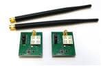
131384-HMC1010LP4E

Analog Devices Inc.
131384-HMC1010LP4E
Analog Devices Inc.
The HMC1010LP4E Power Detector is designed for RF power measurement, and control applications for frequencies up to 3.9 GHz. The detector provides an accurate RMS representation of any RF/IF input signal. The output is a temperature compensated monotonic, representation of real signal power, measured with an input sensing range of 60 dB.The HMC1010LP4E is ideally suited to those wide bandwidth, wide dynamic range applications, requiring repeatable measurement of real signal power, especially where RF/IF wave shape and/or crest factor change with time.The integration bandwidth of the HMC1010LP4E is digitally programmable with the use of input pins SC I1- 4 with a range of more than 4 decades. This allows the user to dynamically set the operation bandwidth providing the capability of handling different types of modulations on the same platform.The HMC1010LP4E features an internal op-amp at output stage, which provides for slope & intercept adjustments and enables controller application.Applications Log ?> Root-Mean-Square?(RMS) Conversion Received Signal Strength?Indication (RSSI) Transmitter Signal Strength?Indication (TSSI) RF Power Amplifier Efficiency Control Receiver Automatic Gain Control Transmitter Power Control
AD8113-EVALZ

Analog Devices Inc.
AD8113-EVALZ
Analog Devices Inc.
The AD8113 is a fully buffered crosspoint switch matrix that operates on ?12V for Audio applications and ?5V for Video applications. It offers a -3dB signal bandwidth greater than 60MHz and channel switch times of less than 60ns with 0.1% settling for use in both analog and digital audio. The AD8113 operated at 20kHz has crosstalk performance of -83dB and isolation of 90dB. In addition, ground/power pins surround all inputs and outputs to provide extra shielding for operation in the most demanding audio routing applications. The differential gain and differential phase of better than 0.1% and 0.1?, respectively, along with 0.1dB flatness out to 10MHz make the AD8113 suitable for many video applications.The AD8113 includes 16 independent output buffers that can be placed into a disabled state for paralleling crosspoint outputs so that off channel loading is minimized. The AD8113 has a gain of +2. It operates on voltage supplies of ?5V or ?12V while consuming only 34mA or 31mA of current, respectively.The channel switching is performed via a serial digital control (which can accommodate daisy-chaining of several devices) or via a parallel control, allowing updating of an individual output without reprogramming the entire array.The AD8113 is packaged in a 100-lead LQFP and is available over the commercial temperature range of 0?C to 70?C.
AD8334-EVALZ

Analog Devices Inc.
AD8334-EVALZ
Analog Devices Inc.
The AD8334 is an ultralow noise, quad channel linear-in-dB variable gain amplifier (VGA). Although optimized for ultrasound systems, it may be used as a low noise variable gain control in any application whose operating frequency is less than 100 MHz.Included in each channel are an ultralow noise preamp (LNA), an X-AMP? VGA with 48 dB of gain range, and a selectable gain postamp with adjustable output limiting. The LNA gain is 19 dB with a single-ended input and differential outputs. Using a single resistor, the LNA input impedance can be adjusted to match a signal source without compromising noise performance.The 48 dB gain range of the VGA makes these devices suitable for a variety of applications. Excellent bandwidth uniformity is maintained across the entire range. The gain control interface provides precise linear-in-dB scaling of 50 dB/V for control voltages between 40 mV and 1 V. Factory trim ensures excellent part-to-part and channel-to-channel gain matching. Differential signal paths result in superb second- and third-order distortion performance and low crosstalk.The AD8334 is a quad version of the single AD8331 and dual AD8332.For information on specs, see the AD8331/AD8332/AD8334 datasheet.Applications Ultrasound and sonar time-gain controls High performance automatic gain control (AGC) systems I/Q signal processing High speed, dual ADC drivers
AD8376-EVALZ

Analog Devices Inc.
AD8376-EVALZ
Analog Devices Inc.
The AD8376 is a dual channel, digitally controlled, variable gain wide bandwidth amplifier that provides precise gain control, high IP3, and low noise figure. The excellent distortion performance and high signal bandwidth make the AD8376 an excellent gain control device for a variety of receiver applications. Using an advanced high speed SiGe process and incorporating proprietary distortion cancellation techniques, the AD8376 achieves 50 dBm output IP3 at 200 MHz. The AD8376 provides a broad 24 dB gain range with 1 dB resolution. The gain of each channel is adjusted through dedicated 5-pin control interfaces and can be driven using standard TTL levels. The open-collector outputs provide a flexible interface, allowing the overall signal gain to be set by the loading impedance. Thus, the signal voltage gain is directly proportional to the load. Each channel of the AD8376 can be individually powered on by applying the appropriate logic level to the ENBA and ENBB power enable pins. The quiescent current of the AD8376 is typically 130 mA per channel. When powered down, the AD8376 consumes less than 5 mA and offers excellent input-to-output isolation, lower than ?50 dB at 200 MHz. Fabricated on an Analog Devices, Inc., high speed SiGe process, the AD8376 is supplied in a compact, thermally enhanced, 5 mm ? 5mm 32-lead LFCSP package and operates over the temperature range of ?40?C to +85?C.ApplicationsDifferential ADC drivers Main and diversity IF sampling receivers Wideband multichannel receivers Instrumentation Data Sheet, Rev. 0, 8/07
AD8556-EVALZ

Analog Devices Inc.
AD8556-EVALZ
Analog Devices Inc.
The AD8556 is a zero-drift, sensor signal amplifier withdigitally programmable gain and output offset. Designed toeasily and accurately convert variable pressure sensor andstrain bridge outputsto a well-defined output voltage range,the AD8556 accurately amplifies many other differential orsingle-ended sensor outputs. The AD8556 uses the ADIpatented low noise auto-zero and DigiTrim? technologies tocreate an incredibly accurate and flexible signal processingsolution in a very compact footprint.Gain is digitally programmable in a wide range from 70 to1,280 through a serial data interface. Gain adjustment canbe fully simulated in-circuit and then permanently programmedwith reliable polyfuse technology. Output offsetvoltage is also digitally programmable and is ratiometric to thesupply voltage. AD8556 also features internal EMI filters on theVNEG, VPOS, FILT and VCLAMP pins.In addition to extremely low input offset voltage, low inputoffset voltage drift, and very high dc and ac CMRR, the AD8556 also includes a pull-up current source at the input pinsand a pull-down current source at the VCLAMP pin. Thisallows open wire and shorted wire fault detection. A low-passfilter function is implemented via a single low cost externalcapacitor. Output clamping set via an external reference voltageallows the AD8556 to drive lower voltage ADCs safely andaccurately.When used in conjunction with an ADC referenced to the samesupply, the system accuracy becomes immune to normal supplyvoltage variations. Output offset voltage can be adjusted with aresolution of better than 0.4% of the difference between VDDand VSS. A lockout trim after gain and offset adjustmentfurther ensures field reliability.The AD8556 is fully specified from ?40?C to +140?C.Operating from single-supply voltages of 2.7 V to 5.5 V, theAD8556 is offered in the 8-lead SOIC_N, and 4 mm ? 4 mm16-lead LFCSP_VQ.ApplicationsAutomotive SensorsPressure and Position SensorsPrecision Current SensingStrain Gages
AD8479R-EBZ

Analog Devices Inc.
AD8479R-EBZ
Analog Devices Inc.
The AD8479 is a difference amplifier with a very high inputcommon-mode voltage range. The AD8479 is a precision devicethat allows the user to accurately measure differential signals inthe presence of high common-mode voltages up to ?600 V.The AD8479 can replace costly isolation amplifiers in applicationsthat do not require galvanic isolation. The device operates overa ?600 V common-mode voltage range and has inputs that areprotected from common-mode or differential mode transientsup to ?600 V.The AD8479 has low offset voltage, low offset voltage drift, low gain drift, low common-mode rejection drift, and excellent common-mode rejection ratio (CMRR) over a wide frequency range.The AD8479 is available in a space-saving 8-lead SOIC package and is operational over the ?40?C to +125?C temperature range.Applications High voltage current sensing Battery cell voltage monitors Power supply current monitors Motor controls Isolation
AD9228-65KITZ
Analog Devices Inc.
AD9228-65KITZ
Analog Devices Inc.
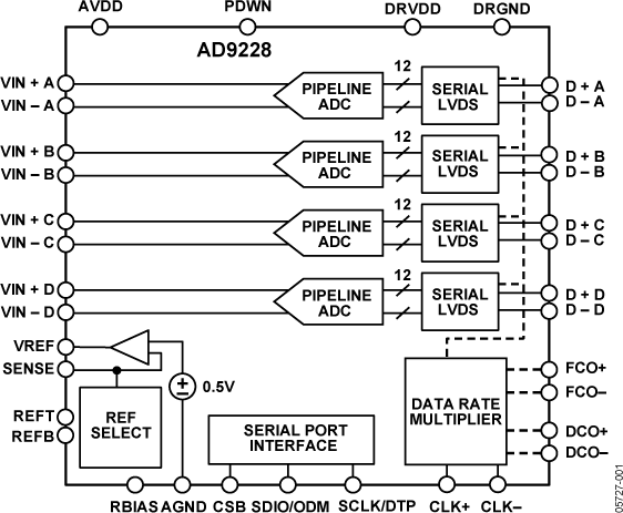
The AD9228 is a quad, 12-bit, 40/65 MSPS analog-to-digital converter (ADC) with an on-chip sample-and-hold circuit designed for low cost, low power, small size, and ease of use. The product operates at a conversion rate of up to 65 MSPS and is optimized for outstanding dynamic performance and low power in applications where a small package size is critical. The ADC requires a single 1.8 V power supply and LVPECL-/ CMOS-/LVDS-compatible sample rate clock for full performance operation. No external reference or driver components are required for many applications. The ADC automatically multiplies the sample rate clock for the appropriate LVDS serial data rate. A data clock output (DCO) for capturing data on the output and a frame clock output (FCO) for signaling a new output byte are provided. Individual channel power-down is supported and typically consumes The ADC contains several features designed to maximize flexibility and minimize system cost, such as programmable clock and data alignment and programmable digital test pattern generation. The available digital test patterns include built-in deterministic and pseudorandom patterns, along with custom user-defined test patterns entered via the serial port interface (SPI). The AD9228 is available in an RoHS compliant, 48-lead LFCSP. It is specified over the industrial temperature range of ?40?C to +85?C.PRODUCT HIGHLIGHTSSmall Footprint. Four ADCs are contained in a small, space-saving package. Low power of 119 mW/channel at 65 MSPS. Ease of Use. A data clock output (DCO) is provided that operates at frequencies of up to 390 MHz and supports double data rate (DDR) operation.User Flexibility. The SPI control offers a wide range of flexible features to meet specific system requirements. Pin-Compatible Family. This includes the AD9287 (8-bit), AD9219 (10-bit), and AD9259 (14-bit).?APPLICATIONSMedical imaging and nondestructive ultrasound Portable ultrasound and digital beam-forming systemsQuadrature radio receivers Diversity radio receivers Tape drives Optical networking Test equipment
AD9520-5/PCBZ

Analog Devices Inc.
AD9520-5/PCBZ
Analog Devices Inc.
The AD9520-5 provides a multioutput clock distributionfunction with subpicosecond jitter performance, along withan on-chip PLL that can be used with an external VCO.The AD9520-5 serial interface supports both SPI and I2C ports.An in-package EEPROM, which can be programmed through theserial interface, can store user-defined register settings forpower-up and chip reset.The AD9520-5 features 12 LVPECL outputs in four groups. Anyof the 1.6 GHz LVPECL outputs can be reconfigured as two250 MHz CMOS outputs. If an application requires LVDSdrivers instead of LVPECL drivers, refer to the AD9522-5.Each group of three outputs has a divider that allows both thedivide ratio (from 1 to 32) and the phase offset or coarse timedelay to be set.The AD9520-5 is available in a 64-lead LFCSP and can be operatedfrom a single 3.3 V supply. The external VCO can have anoperating voltage of up to 5.5 V. A separate output driver powersupply can be from 2.375 V to 3.465 V.The AD9520-5 is specified for operation over the standardindustrial range of ?40?C to +85?C. Applications Low jitter, low phase noise clock distribution Clock generation and translation for SONET, 10Ge, 10GFC, Synchronous Ethernet, OTU2/3/4 Forward error correction (G.710) Clocking high speed ADCs, DACs, DDSs, DDCs, DUCs, MxFEs High performance wireless transceivers ATE and high performance instrumentation Broadband infrastructures
AD9517-3A/PCBZ

Analog Devices Inc.
AD9517-3A/PCBZ
Analog Devices Inc.
The AD9517-31 provides a multi-output clock distribution function with subpicosecond jitter performance, along with an on-chip PLL and VCO. The on-chip VCO tunes from 1.75 GHz to 2.25 GHz. Optionally, an external VCO/VCXO of up to 2.4 GHz can be used.The AD9517-3 emphasizes low jitter and phase noise to maximize data converter performance, and it can benefit other applications with demanding phase noise and jitter requirements.The AD9517-3 features four LVPECL outputs (in two pairs) and four LVDS outputs (in two pairs). Each LVDS output can be reconfigured as two CMOS outputs. The LVPECL outputs operate to 1.6 GHz, the LVDS outputs operate to 800 MHz, and the CMOS outputs operate to 250 MHz.For applications that require additional outputs, a crystal reference input, zero-delay, or EEPROM for automatic configuration at startup, the AD9520 and AD9522 are available. In addition, the AD9516 and AD9518 are similar to the AD9517 but have a different combination of outputs.Each pair of outputs has dividers that allow both the divide ratio and coarse delay (or phase) to be set. The range of division for the LVPECL outputs is 1 to 32. The LVDS/CMOS outputs allow a range of divisions up to a maximum of 1024.The AD9517-3 is available in a 48-lead LFCSP and can be operated from a single 3.3 V supply. An external VCO, which requires an extended voltage range, can be accommodated by connecting the charge pump supply (VCP) to 5 V. A separate LVPECL power supply can be from 2.5 V to 3.3 V (nominal).The AD9517-3 is specified for operation over the industrial range of ?40?C to +85?C.APPLICATIONS Low jitter, low phase noise clock distribution 10/40/100 Gb/sec networking line cards, including SONET, Synchronous Ethernet, OTU2/3/4 Forward error correction (G.710) Clocking high speed ADCs, DACs, DDSs, DDCs, DUCs, MxFEs High performance wireless transceivers ATE and high performance instrumentation 1 AD9517 is used throughout to refer to all the members of the AD9517 family. However, when AD9517-3 is used, it is referring to that specific member of the AD9517 family.
AD9671EBZ

Analog Devices Inc.
AD9671EBZ
Analog Devices Inc.
The AD9671 is designed for low cost, low power, small size, andease of use for medical ultrasound applications. It contains eightchannels of a VGA with an LNA, a CW harmonic rejection I/Qdemodulator with programmable phase rotation, an AAF, anADC, and a digital demodulator and decimator for dataprocessing and bandwidth reduction.Each channel features a maximum gain of up to 52 dB, a fullydifferential signal path, and an active input preamplifier termination.The channel is optimized for high dynamic performance andlow power in applications where a small package size is critical.The LNA has a single-ended to differential gain that is selectablethrough the serial port interface (SPI). Assuming a 15 MHz noisebandwidth (NBW) and a 21.6 dB LNA gain, the LNA input SNRis 94 dB. In CW Doppler mode, each LNA output drives an I/Qdemodulator that has independently programmable phaserotation with 16 phase settings.Power-down of individual channels is supported to increasebattery life for portable applications. Standby mode allows quickpower-up for power cycling. In CW Doppler operation, theVGA, AAF, and ADC are powered down. The ADC containsseveral features designed to maximize flexibility and minimizesystem cost, such as a programmable clock, data alignment, andprogrammable digital test pattern generation. The digital testpatterns include built-in fixed patterns, built-in pseudorandompatterns, and custom user defined test patterns entered via the SPI.Applications Medical imaging/ultrasound Nondestructive testing (NDT)
AD9648-125EBZ

Analog Devices Inc.
AD9648-125EBZ
Analog Devices Inc.
The AD9648 is a monolithic, dual-channel, 1.8 V supply, 14-bit, 105 MSPS/125 MSPS analog-to-digital converter (ADC). It features a high performance sample-and-hold circuit and on-chip voltage reference. The product uses multistage differential pipeline architecture with output error correction logic to provide 14-bit accuracy at 125 MSPS data rates and to guarantee no missing codes over the full operating temperature range.The ADC contains several features designed to maximize flexibility and minimize system cost, such as programmable clock and data alignment and programmable digital test pattern generation. The available digital test patterns include built-in deterministic and pseudorandom patterns, along with custom user-defined test patterns entered via the serial port interface (SPI).A differential clock input controls all internal conversion cycles. An optional duty cycle stabilizer (DCS) compensates for wide variations in the clock duty cycle while maintaining excellent overall ADC performance.The digital output data is presented in offset binary, Gray code, or twos complement format. A data output clock (DCO) is provided for each ADC channel to ensure proper latch timing with receiving logic. Output logic levels of 1.8 V CMOS or LVDS are supported. Output data can also be multiplexed onto a single output bus.The AD9648 is available in a 64-lead RoHS compliant LFCSP and is specified over the industrial temperature range (?40?C to +85?C). Applications Communications Diversity radio systems Multimode digital receivers GSM, EDGE, W-CDMA, LTE, CDMA2000, WiMAX, TD-SCDMA I/Q demodulation systems Smart antenna systems Broadband data applications Battery-powered instruments Hand held scope meters Portable medical imaging Ultrasound Radar/LIDARProduct Highlights The AD9648 operates from a single 1.8 V analog power supply and features a separate digital output driver supply to accommodate 1.8 V CMOS or LVDS logic families. The patented sample-and-hold circuit maintains excellent performance for input frequencies up to 200 MHz and is designed for low cost, low power, and ease of use. A standard serial port interface supports various product features and functions, such as data output formatting, internal clock divider, power-down, DCO/data timing and offset adjustments. The AD9648 is packaged in a 64-lead RoHS compliant LFCSP that is pin compatible with the AD9650/AD9269/AD9268 16-bit ADC?s, the AD9258 14-bit ADC, the AD9628/AD9231 12-bit ADC?s, and the AD9608/AD9204 10-bit ADC?s, enabling a simple migration path between 10-bit and 16-bit converters sampling from 20 MSPS to 125 MSPS.
AD9633-125EBZ

Analog Devices Inc.
AD9633-125EBZ
Analog Devices Inc.
The AD9633 is a quad, 12-bit, 80 MSPS/105 MSPS/125 MSPS analog-to-digital converter (ADC) with an on-chip sample-and-hold circuit designed for low cost, low power, small size, and ease of use. The product operates at a conversion rate of up to 125 MSPS and is optimized for outstanding dynamic performance and low power in applications where a small package size is critical.The ADC requires a single 1.8 V power supply and LVPECL-/CMOS-/LVDS-compatible sample rate clock for full performance operation. No external reference or driver components are required for many applications.The ADC automatically multiplies the sample rate clock for the appropriate LVDS serial data rate. A data clock output (DCO) for capturing data on the output and a frame clock output (FCO) for signaling a new output byte are provided. Individual-channel power-down is supported and typically consumes less than 2 mW when all channels are disabled.The ADC contains several features designed to maximize flexibility and minimize system cost, such as programmable output clock and data alignment and digital test pattern generation. The available digital test patterns include built-in deterministic and pseudorandom patterns, along with custom user-defined test patterns entered via the serial port interface (SPI).The AD9633 is available in a RoHS-compliant, 48-lead LFCSP. It is specified over the industrial temperature range of ?40?C to +85?C. This product is protected by a U.S. patent. Applications Medical ultrasound High speed imaging Quadrature radio receivers Diversity radio receivers Test equipment
AD9959/PCBZ

Analog Devices Inc.
AD9959/PCBZ
Analog Devices Inc.
The AD9959 consists of four direct digital synthesizer (DDS)cores that provide independent frequency, phase, and amplitudecontrol on each channel. This flexibility can be used to correct imbalances between signals due to analog processing, such asfiltering, amplification, or PCB layout-related mismatches.Because all channels share a common system clock, they areinherently synchronized. Synchronization of multiple devices is supported.The AD9959 can perform up to a 16-level modulation of fre-quency, phase, or amplitude (FSK, PSK, ASK). Modulation isperformed by applying data to the profile pins. In addition, theAD9959 also supports linear sweep of frequency, phase, or amplitude for applications such as radar and instrumentation. The AD9959 serial I/O port offers multiple configurations to provide significant flexibility. The serial I/O port offers an SPI-compatible mode of operation that is virtually identical to the SPI operation found in earlier Analog Devices, Inc., DDS products. Flexibility is provided by four data pins (SDIO_0/SDIO_1/SDIO_2/SDIO_3) that allow four programmable modes of serial I/O operation.The AD9959 uses advanced DDS technology that provides low power dissipation with high performance. The device incorporates four integrated, high speed 10-bit DACs with excellent wideband and narrow-band SFDR. Each channel has a dedicated 32-bit frequency tuning word, 14 bits of phase offset, and a 10-bit output scale multiplier. The DAC outputs are supply referenced and must be terminated into AVDD by a resistor or an AVDD center-tapped transformer. Each DAC has its own programmable reference to enable different full-scale currents for each channel. The DDS acts as a high resolution frequency divider with the REFCLK as the input and the DAC providing the output. The REFCLK input source is common to all channels and can be driven directly or used in combination with an integrated REFCLK multiplier (PLL) up to a maximum of 500 MSPS. The PLL multiplication factor is programmable from 4 to 20, in integer steps. The REFCLK input also features an oscillator circuit to support an external crystal as the REFCLK source. The crystal must be between 20 MHz and 30 MHz. The crystal can be used in combination with the REFCLK multiplier.The AD9959 comes in a space-saving 56-lead LFCSP package. The DDS core (AVDD and DVDD pins) is powered by a 1.8 V supply. The digital I/O interface (SPI) operates at 3.3 V and requires DVDD_I/O (Pin 49) be connected to 3.3 V. The AD9959 operates over the industrial temperature range of ?40?C to +85?C.APPLICATIONSAgile local oscillators Phased array radars/sonars Instrumentation Synchronized clocking RF source for AOTF
ADA4891-3AR-EBZ

Analog Devices Inc.
ADA4891-3AR-EBZ
Analog Devices Inc.
The ADA4891-1 (single), ADA4891-2 (dual), ADA4891-3 (triple), and ADA4891-4 (quad) are CMOS, high speed amplifiers that offer high performance at a low cost. The amplifiers feature true single-supply capability, with an input voltage range that extends 300 mV below the negative rail.In spite of their low cost, the ADA4891 family provides high performance and versatility. The rail-to-rail output stage enables the output to swing within 50 mV of each rail, enabling maximum dynamic range.The ADA4891 family of amplifiers is ideal for imaging applications, such as consumer video, CCD buffers, and contact image sensor buffers. Low distortion and fast settling time also make them ideal for active filter applications.The ADA4891-1/ADA4891-2/ADA4891-3/ADA4891-4 are available in a wide variety of packages.The ADA4891-1 is available in 8-lead SOIC and 5-lead SOT-23 packages.The ADA4891-2 is available in 8-lead SOIC and 8-lead MSOP packages.The ADA4891-3 and ADA4891-4 are available in 14-lead SOIC and 14-lead TSSOP packages.The amplifiers are specified to operate over the extended temperature range of ?40?C to +125?C.Applications Imaging Consumer video Active filters Coaxial cable drivers Clock buffers Photodiode preamp Contact image sensor and buffers
ADA8282CP-EBZ

Analog Devices Inc.
ADA8282CP-EBZ
Analog Devices Inc.
The ADA8282 is designed for applications that require low cost, low power, compact size, and flexibility. The ADA8282 has four parallel channels, each including a low noise preamplifier (LNA) and a programmable gain amplifier (PGA). The LNA and PGA combine to form a signal chain that features a gain range of 18 dB to 36 dB in 6 dB increments with a guaranteed minimum bandwidth of 5 MHz.Using the highest power settings, the combined input referred voltage noise of the combined LNA and PGA channel is 3.4 nV/?Hz at maximum gain. The ADA8282 can be configured in four power modes that trade off power and noise performance to optimize the performance according to the end application. Fabricated in an advanced complementary metal-oxide semiconductor (CMOS) process, the ADA8282 is available in a 5 mm ? 5 mm, RoHS-compliant, 32-lead LFCSP. It is specified over the automotive temperature range of ?40?C to +125?C. Applications Automotive radar Adaptive cruise control Collision avoidance Blind spot detection Self parking Electronic bumper
ADAR1000EVAL1Z

Analog Devices Inc.
ADAR1000EVAL1Z
Analog Devices Inc.
The ADAR1000 is a 4-channel, X and Ku frequency band, beamforming core chip for phased arrays. This device operates in half-duplex between receive and transmit modes. In receive mode, input signals pass through four receive channels and are combined and output at the common RF_IO pin. In transmit mode, the RF_IO input signal is split and passes through the four transmit channels. In both modes, the ADAR1000 provides a ?31 dB gain adjustment range and a full 360? phase adjustment range in each radio frequency (RF) channel, with 6-bit resolution (less than ?0.5 dB and 2.8?, respectively).A simple 4-wire serial port interface (SPI) controls all of the on-chip registers. In addition, two address pins allow SPI control of up to four devices on the same serial lines. Dedicated transmit and receive load pins also provide synchronization of all ADAR1000 chips in the same array, and a single pin controls fast switching between the transmit and receive modes. The ADAR1000 is fabricated in a silicon-germanium, bipolar CMOS (BiCMOS) process. The device is available in a compact, 88-terminal, 7 mm ? 7 mm, LGA package and is specified from ?40?C to +85?C.APPLICATIONS Phased array radar Satellite communications systems
ADA4433-1BCP-EBZ

Analog Devices Inc.
ADA4433-1BCP-EBZ
Analog Devices Inc.
The ?ADA4433-1 is a differential output, fully integrated video reconstruction filter that combines overvoltage protection (short-to-battery [STB] protection) and short-to-ground (STG) protection on the outputs, with excellent video specifications and low power consumption. The combination of STB protection and robust ESD tolerance allows the ADA4433-1 to provide superior protection in the hostile automotive environment.The ADA4433-1 is a fully differential video filter that can be used as a fully differential input to a differential output or as a single-ended input to a differential output, allowing it to easily connect to both differential and single-ended sources. It is capable of driving twisted pair or coaxial cable with minimal line attenuation. Differential signal processing reduces the effects of ground noise, which can plague ground referenced systems. The ADA4433-1 is ideal for differential signal processing (gain and filtering) throughout the signal chain, simplifying the conversion between single-ended and differential components.The short-to-battery protection integrated into the ADA4433-1 protects against both dc and transient overvoltage events, caused by an accidental short to a battery voltage up to 18 V. The Analog Devices, Inc., short-to-battery protection eliminates the need for large output coupling capacitors and other complicated circuits used to protect standard video amplifiers, saving space and cost.The ADA4433-1 features a high-order filter with ?3 dB cutoff frequency response at 10 MHz and 45 dB of rejection at 27 MHz. The ADA4433-1 featurea an internally fixed gain of 2 V/V. This makes the ADA4433-1 ideal for SD video applications, including NTSC and PAL.The ADA4433-1 operates on single supplies as low as 2.6 V and as high as 3.6 V while providing the dynamic range required by the most demanding video systems.The ADA4433-1 is offered in an 8-lead, 3 mm ? 3 mm LFCSP package, rated for operation over the wide automotive temperature range of ?40?C to +125?C.Appplications Automotive rearview cameras Automotive video electronic control units (ECUs) Surveillance video systems
ADIS16477-1/PCBZ

Analog Devices Inc.
ADIS16477-1/PCBZ
Analog Devices Inc.
The ADIS16477 is a precision, miniature MEMS inertial measurement unit (IMU) that includes a triaxial gyroscope and a triaxial accelerometer. Each inertial sensor in the ADIS16477 combines with signal conditioning that optimizes dynamic performance. The factory calibration characterizes each sensor for sensitivity, bias, alignment, linear acceleration (gyroscope bias), and point of percussion (accelerometer location). As a result, each sensor has dynamic compensation formulas that provide accurate sensor measurements over a broad set of conditions.The ADIS16477 provides a simple, cost effective method for integrating accurate, multiaxis inertial sensing into industrial systems, especially when compared with the complexity and investment associated with discrete designs. All necessary motion testing and calibration are part of the production process at the factory, greatly reducing system integration time. Tight orthogonal alignment simplifies inertial frame alignment in navigation systems. The serial peripheral interface (SPI) and register structure provide a simple interface for data collection and configuration control.The ADIS16477 is available in a 44-ball, ball grid array (BGA) package that is approximately 11 mm ? 15 mm ? 11 mm.Applications Navigation, stabilization, and instrumentation Unmanned and autonomous vehicles Smart agriculture/construction machinery Factory/industrial automation, robotics Virtual/augmented reality Internet of Moving Things
ADL5387-EVALZ

Analog Devices Inc.
ADL5387-EVALZ
Analog Devices Inc.
The ADL5387 is a broadband quadrature I/Q demodulator that covers an RF/IF input frequency range from 30 MHz to 2 GHz. With a NF = 13.2 dB, IP1dB = 12.7 dBm, and IIP3 = 32 dBm @ 450 MHz, the ADL5387 demodulator offers outstanding dynamic range suitable for the demanding infrastructure direct-conversion requirements. The differential RF/IF inputs provide a well-behaved broadband input impedance of 50 ? and are best driven from a 1:1 balun for optimum performance.Ultrabroadband operation is achieved with a divide-by-2 method for local oscillator (LO) quadrature generation. Over a wide range of LO levels, excellent demodulation accuracy is achieved with amplitude and phase balances ~0.05 dB and ~0.4?, respectively. The demodulated in-phase (I) and quadrature (Q) differential outputs are fully buffered and provide a voltage conversion gain of >4 dB. The buffered baseband outputs are capable of driving a 2 Vp-p differential signal into 200 ?.The fully balanced design minimizes effects from second-order distortion. The leakage from the LO port to the RF port is 60 dBm.The ADL5387 operates off a single 4.75 V to 5.25 V supply. The supply current is adjustable with an external resistor from the BIAS pin to ground.The ADL5387 is fabricated using the Analog Devices, Inc. advanced silicon-germanium bipolar process and is available in a 24-lead exposed paddle LFCSP.APPLICATIONS QAM/QPSK RF/IF demodulators W-CDMA/CDMA/CDMA2000/GSM Microwave point-to-(multi)point radios Broadband wireless and WiMAX Broadband CATVs