
KSZ9031MNX-EVAL
Microchip Technology Inc.Ethernet Development Tools 1-Port Gigabit Ethernet PHY - Evaluation Board
EVALPASCO2SENSOR2GOTOBO1
Infineon Technologies AGMultiple Function Sensor Development Tools Design-in & prototyping Easy connection to application board
EVAL6EDL7141TRAP1SHTOBO1
Infineon Technologies AG6EDL7141 Gate Driver Power Management Evaluation Board

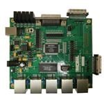
KSZ8863FLL-EVAL
Microchip Technology Inc.Ethernet Development Tools 3-Port 10/100 Ethernet Switch with 1x FX Port and 1x TX Port - Evaluation Board
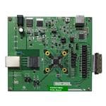
KSZ8091RNA-EVAL
Microchip Technology Inc.Ethernet Development Tools Eval - 10/100 PHY w/EEE & WOL, 0.11u
KSZ8081RNB-EVAL
Microchip Technology Inc.Ethernet Development Tools 10/100 PHY, 0.11u - Evaluation Board
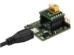
KSZ9031RNX-EVAL
Microchip Technology Inc.Ethernet Development Tools 1-Port Gigabit Ethernet PHY - Evaluation Board
KSZ8863FLL-EVAL
Microchip Technology Inc.Ethernet Development Tools 3-Port 10/100 Ethernet Switch with 1x FX Port and 1x TX Port - Evaluation Board


