INA250 Current Shunt Monitor Evaluation Module
Texas InstrumentsINA250 Current Shunt Monitor Evaluation Module
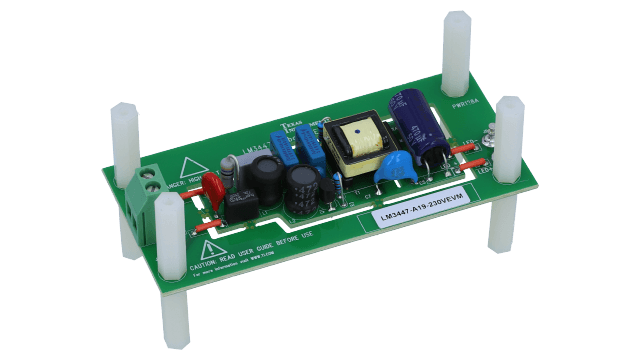
LM3447 Flyback Controller for LED Lighting Evaluation Module Board
Texas InstrumentsLM3447 Flyback Controller for LED Lighting Evaluation Module Board

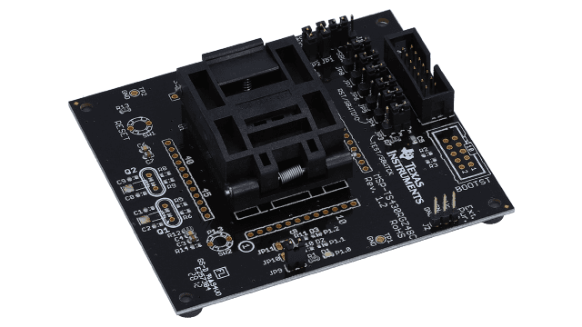
MSP-TS430RGZ48C - 48-pin Target Development Board for MSP430FRxx FRAM MCUs
Texas InstrumentsMSP-TS430RGZ48C - 48-pin Target Development Board for MSP430FRxx FRAM MCUs
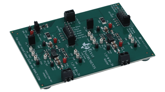
Evaluation Module for TPS53311 Synchronous Step Down DCDC Converter
Texas InstrumentsEvaluation Module for TPS53311 Synchronous Step Down DCDC Converter
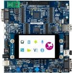
STM32479I-EVAL
STMicroelectronicsEvaluation Board, STM32F479NI MCU, SPI/I2C Interfaces, Integrated ST-LINK/V2-1 Debugger

HD3SS460EVM-SRC high-speed passive crosspoint switch evaluation module
Texas InstrumentsHD3SS460EVM-SRC high-speed passive crosspoint switch evaluation module


