Multi-Display Inductorless LED Driver with 32 Exponential Dimming Steps in micro SMD
Texas InstrumentsMulti-Display Inductorless LED Driver with 32 Exponential Dimming Steps in micro SMD
Evaluation Module for TPS62615 350-mA, 6-MHz, 1.2Vout High Efficiency Step-Down Converter
Texas InstrumentsEvaluation Module for TPS62615 350-mA, 6-MHz, 1.2Vout High Efficiency Step-Down Converter
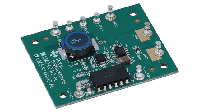
LM3404HVMA (SOIC) - 1A Constant Current Buck HV Regulator for HB LEDs (LM3404HVEVAL Board)
Texas InstrumentsLM3404HVMA (SOIC) - 1A Constant Current Buck HV Regulator for HB LEDs (LM3404HVEVAL Board)
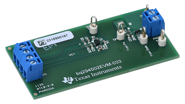
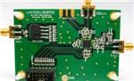
bq294502 Voltage Protector for 2-Series or 3-Series Cell Li-Ion Batteries EVM
Texas Instrumentsbq294502 Voltage Protector for 2-Series or 3-Series Cell Li-Ion Batteries EVM
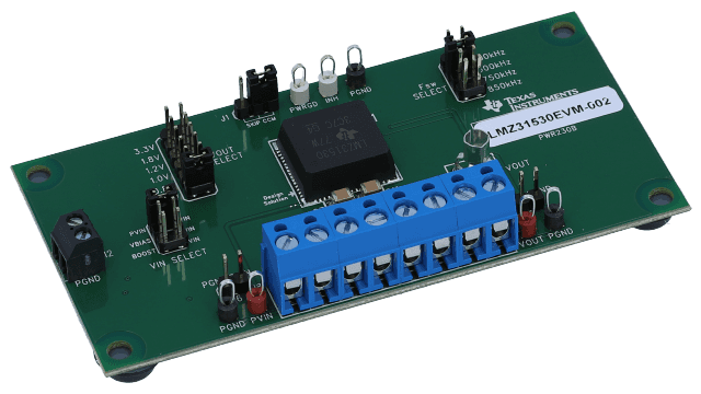
LMZ31530 3V to 14.5V; 30A Step-Down Power Module Evaluation Board
Texas InstrumentsLMZ31530 3V to 14.5V; 30A Step-Down Power Module Evaluation Board
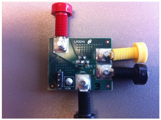
LM3241TLEVAL 6MHz, 750mA Miniature, Adjustable, Step-Down DC-DC Converter for RF Power Amplifiers
Texas InstrumentsLM3241TLEVAL 6MHz, 750mA Miniature, Adjustable, Step-Down DC-DC Converter for RF Power Amplifiers
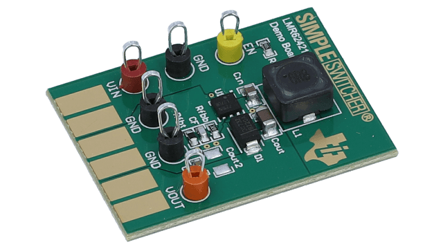
LMR62421 SIMPLE SWITCHER® 24Vout; 2.1A Small Step-Up Regulator Demo Board
Texas InstrumentsLMR62421 SIMPLE SWITCHER® 24Vout; 2.1A Small Step-Up Regulator Demo Board
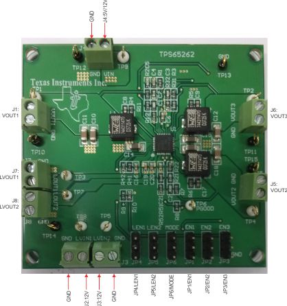
TPS65262 18V Input; Triple 3A/1A/1A Buck Converter with Dual 200mA/100mA LDO Evaluation Module
Texas InstrumentsTPS65262 18V Input; Triple 3A/1A/1A Buck Converter with Dual 200mA/100mA LDO Evaluation Module
4A, PowerWise? Synchronous Buck Regulator with Input Synchronization Evaluation Module
Texas Instruments4A, PowerWise? Synchronous Buck Regulator with Input Synchronization Evaluation Module
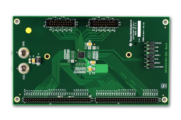
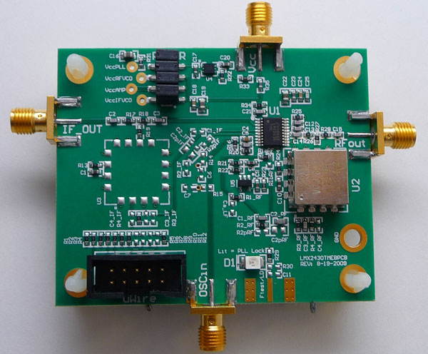
High Performance Frequency Synthesizer System with Integrated VCO
Texas InstrumentsHigh Performance Frequency Synthesizer System with Integrated VCO
LM3444 -230VAC, 8W Isolated Flyback LED Driver (no dim) Evaluation Board
Texas InstrumentsLM3444 -230VAC, 8W Isolated Flyback LED Driver (no dim) Evaluation Board
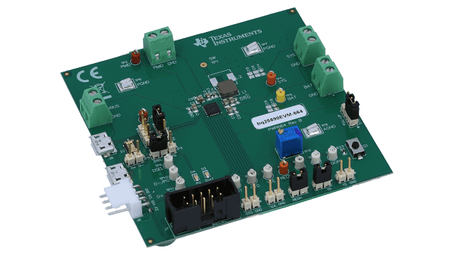
BQ25890 Complete Charger Evaluation Module
Texas InstrumentsBQ25890 Complete Charger Evaluation Module
2.5A, Singe Input, Single Cell Switchmode Li-Ion Battery Charger Evaluation Module
Texas Instruments2.5A, Singe Input, Single Cell Switchmode Li-Ion Battery Charger Evaluation Module
5.0 GHz 2.5 GHz PLLatinum Low Power Dual Frequency Synthesizer for RF Personal Communications
Texas Instruments5.0 GHz 2.5 GHz PLLatinum Low Power Dual Frequency Synthesizer for RF Personal Communications
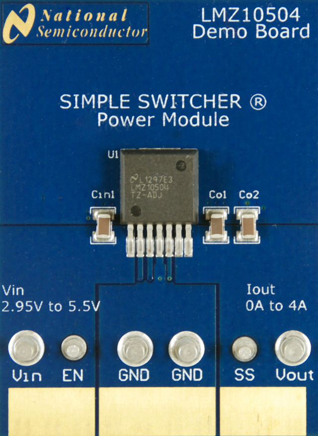
Simple Switcher® Power Module 5.5Vin; 4A Demonstration Board
Texas InstrumentsSimple Switcher® Power Module 5.5Vin; 4A Demonstration Board