Top Manufacturers
MORE
Stock

Displaying 301 - 320 of 12848

Evaluation Kits

EVAL-AD5258DBZ

Analog Devices Inc.
The AD5258 provides a compact, nonvolatile 3 mm ? 4.9 mm packaged solution for 64-position adjustment applications. These devices perform the same electronic adjustment function as mechanical potentiometers?or variable resistors, but with enhanced resolution and solid-state reliability.The wiper settings are controllable through an I2C-compatible digital interface that is also used to read back the wiper register and EEPROM content in addition, resistor tolerance is stored within EEPROM, providing an end-to-end tolerance accuracy of 0.1%. There is also a software write protection function that ensures data cannot be written to the EEPROM register.A separate VLOGIC pin delivers increased interface flexibility. For users who need multiple parts on one bus, Address Bit AD0 and Address Bit AD1 allow up to four devices on the same bus.APPLICATIONS LCD panel VCOM adjustment LCD panel brightness and contrast control Mechanical potentiometer replacement in new designs Programmable power supplies RF amplifier biasing Automotive electronics adjustment Gain control and offset adjustment Fiber to the home systems Electronics level settings

EVAL-AD5270SDZ

Analog Devices Inc.
The AD5270 /?AD5271 are single-channel, 1024-/256-position digital rheostats that combine industry leading variable resistor performance with nonvolatile memory (NVM) in a compact package.The AD5270 / AD5271 ensure less than 1% end-to-end resistor tolerance error and offer 50-times programmable (50-TP) memory.The guaranteed industry leading low resistor tolerance error feature simplifies open-loop applications as well as precision calibration and tolerance matching applications.The AD5270 / AD5271 device wiper settings are controllable through the SPI digital interface. Unlimited adjustments are allowed before programming the resistance value into the 50-TP memory. The AD5270/AD5271 do not require any external voltage supply to facilitate fuse blow and there are 50 opportunities for permanent programming. During 50-TP activation, a permanent blow fuse command freezes the resistance position (analogous to placing epoxy on a mechanical trimmer).The AD5270 / AD5271 are available in a 3 mm x 3 mm, 10-lead LFCSP package and in a 10-lead MSOP package. The parts are guaranteed to operate over the extended industrial temperature range of ?40?C to +125?C.APPLICATIONS Mechanical potentiometer replacements Op-amp: variable gain control Instrumentation: gain, offset adjustment Programmable voltage-to-current conversions Programmable filters, delays, time constants Programmable power supply Sensor calibration

EVAL-AD5311RDBZ

Analog Devices Inc.
The AD5310R?/ AD5311R, members of the nanoDAC? family, are low power, single-channel, 10-bit buffered voltage-out DACs. The devices include a 2.5 V, 2 ppm/?C internal reference. The output span can be programmed to be 0 V to VREF or 0 V to 2 ? VREF. All devices operate from a single 2.7 V to 5.5 V supply and are guaranteed monotonic by design. The devices are available in 10-lead MSOP packages.The AD5310R / AD5311R also incorporate a power-on resetcircuit that ensures that the DAC output powers up to zeroscaleand remains there until a valid write takes place. Thedevice contains a power-down feature that reduces the currentconsumption of the device to 2 ?A at 5 V while in power-downmode.The AD5310R / AD5311R use a versatile SPI or I2C interface,including an asynchronous RESET pin and a VLOGIC pin, allowing 1.8 V compatibility.PRODUCT HIGHLIGHTS High Relative Accuracy (INL): ?0.5 LSB maximum. Low Drift 2.5 V On-Chip Reference: 5 ppm/?C maximum temperature coefficient.APPLICATIONS Process controls Data acquisition systems Digital gain and offset adjustment Programmable voltage sources Optical modules

EVAL-AD5339DBZ

Analog Devices Inc.
The AD5337?/?AD5338?/ AD5339 are dual 8-, 10-, and 12-bit buffered voltage output DACs, respectively. Each part is housed in an 8-lead MSOP package and operates from a single 2.5 V to 5.5 V supply, consuming 250 ?A at 3 V. On-chip output amplifiers allow rail-to-rail output swing with a slew rate of 0.7 V/?s. A 2-wire serial interface operates at clock rates up to 400 kHz. This interface is SMBus compatible at VDD < 3.6 V. Multiple devices can be placed on the same bus.The references for the two DACs are derived from one reference pin. The outputs of all DACs can be updated simultaneously using the software LDAC function. The parts incorporate a power-on reset circuit to ensure that the DAC outputs power up to 0 V and remain there until a valid write to the device takes place. A software clear function resets all input and DAC registers to 0 V. A power-down feature reduces the current consumption of the devices to 200 nA @ 5 V (80 nA @ 3 V).The low power consumption of these parts in normal operation makes them ideally suited to portable battery-operated equipment. The power consumption is typically 1.5 mW at 5 V and 0.75 mW at 3 V, reducing to 1 ?W in power-down mode.APPLICATIONS Portable battery-powered instruments Digital gain and offset adjustment Programmable voltage and current sources Programmable attenuators Industrial process control

EVAL-AD5344DBZ

Analog Devices Inc.
The AD5334/AD5335/AD5336/AD5344 are quad 8-,10-,and 12-bit DACs. They operate from a 2.5 V to 5.5 V supply consuming just 500 ?A at 3 V, and feature a power-down mode that further reduces the current to 80 nA. These devices incorporate an on-chip output buffer that can drive the output to both supply rails.PRODUCT HIGHLIGHTS Available in a 28-lead TSSOP package Low power, single supply operation from 2.5 V to 5.5 V supply Consumes 1.5 mW at 3 V and 3 mW at 5 V On-chip ouput buffer can drive output to both supply rails

EVAL-AD5413SDZ

Analog Devices Inc.
The AD5413 is a single-channel, 14-bit voltage and current output, digital-to-analog converter (DAC) that operates within a power supply range from a ?33 V minimum on the AVSS pin to a +33 V maximum on the AVDD1 pin. The CHART pin enables a highway addressable remote transducer (HART?) signal to be ac-coupled on the current output.The AD5413 uses a versatile, 4-wire serial peripheral interface (SPI) that operates at clock rates of up to 50 MHz and is compatible with standard SPI, QSPI?, MICROWIRE?, digital signal processor (DSP), and microcontroller interface standards. The SPI interface has an optional SPI cyclic redundancy check (CRC). The AD5413 implements improved diagnostic features from earlier versions of similar DACs.APPLICATIONS Process control Actuator control Channel isolated analog outputs Programmable logic controller (PLC) and distributed control systems (DCS) applications HART network connectivity

EVAL-AD5422LFEBZ

Analog Devices Inc.
The AD5412/AD5422 are low cost, precision, fully integrated12-/16-bit digital-to-analog converters (DAC) offering a programmable current source and programmable voltage output designed to meet the requirements of industrial process control applications.The output current range is programmable at 4 mA to 20 mA, 0 mA to 20 mA, or an overrange function of 0 mA to 24 mA.The LFCSP version of this product has a CAP2 pin so that the HART signals can be coupled onto the current output of the AD5412/AD5422.Voltage output is provided from a separate pin that can be configured to provide 0 V to 5 V, 0 V to 10 V, ?5 V, or ?10 V output ranges; an overrange of 10% is available on all ranges.Analog outputs are short and open-circuit protected and can drive capacitive loads of 1 ?F.The device operates with an AVDD power supply range from 10.8 V to 40 V. Current loop compliance voltage is 0 V to AVDD ? 2.5 V.The flexible serial interface is SPI- and MICROWIRE?-compatible and can be operated in 3-wire mode to minimize the digital isolation required in isolated applications.The device also includes a power-on-reset function, ensuring that the device powers up in a known state. The part also includes an asynchronous clear pin (CLEAR) that sets the outputs to zero-scale/midscale voltage output or the low end of the selected current range.The total output error is typically ?0.01% in current mode and ?0.01% in voltage mode.Applications Process controls Actuator controls PLC HART network connectivity (LFCSP package only)

EVAL-AD5423SDZ

Analog Devices Inc.
The AD5423 is a single-channel, voltage and current output digital-to-analog converter (DAC) that operates with a power supply range from ?33 V minimum on AVSS to +33 V maximum on AVDD1. The CHART pin enables a Highway Addressable Remote Transducer? (HART) signal to be coupled on the current output. The AD5423 uses a versatile, 4-wire, serial peripheral interface (SPI) that operates at clock rates of up to 50 MHz and is compatible with standard SPI, QSPI?, MICROWIRE?, digital signal processor (DSP), and microcontroller interface standards. The interface also features an optional SPI cyclic redundancy check (CRC) and a watchdog timer (WDT). The AD5423 offers improved diagnostic features from earlier versions of similar DACs, such as an integrated, 12-bit diagnostic analog-to-digital converter (ADC).Product Highlights 16-bit performance. Range of diagnostic features. Integrated 12-bit monitoring ADC. HART compliant.Applications Process control Actuator control Channel isolated analog outputs Programmable logic controller (PLC) and distributed control systems (DCS) applications HART network connectivity

EVAL-AD5445SDZ

Analog Devices Inc.
The AD5424?/?AD5433?/ AD5445 are CMOS 8-, 10-, and 12-bitcurrent output digital-to-analog converters (DACs), respectively.These devices operate from a 2.5 V to 5.5 V power supply,making them suitable for battery-powered applications andmany other applications. These DACs utilize data readback,allowing the user to read the contents of the DAC register viathe DB pins. On power-up, the internal register and latches arefilled with 0s and the DAC outputs are at zero scale.As a result of manufacturing with a CMOS submicron process,they offer excellent 4-quadrant multiplication characteristics,with large signal multiplying bandwidths of up to 10 MHz.The applied external reference input voltage (VREF) determines thefull-scale output current. An integrated feedback resistor (RFB)provides temperature tracking and full-scale voltage outputwhen combined with an external I-to-V precision amplifier.While these devices are upgrades of the AD5424 / AD5433 /AD5445 in multiplying bandwidth performance, they have alatched interface and cannot be used in transparent mode.The AD5424 is available in a small, 20-lead LFCSP and a small,16-lead TSSOP, while the AD5433 and AD5445 DACs are availablein a small, 20-lead LFCSP and a small, 20-lead TSSOP.The EVAL-AD5445SDZ evaluation board is available forevaluating DAC performance. For more information, see theUG-333 evaluation board user guide.APPLICATIONS Portable battery-powered applications Waveform generators Analog processing Instrumentation applications Programmable amplifiers and attenuators Digitally controlled calibration Programmable filters and oscillators Composite video Ultrasound Gain, offset, and voltage trimming

EVAL-AD5590EBZ

Analog Devices Inc.
The AD5590 is a 16-channel input and 16-channel output analog I/O port with eight uncommitted amplifiers, operating from a single 4.5 V to 5.25 V supply. The AD5590 comprises 16 input channels multiplexed into a 1 MSPS, 12-bit successive approximation ADC with a sequencer to allow a preprogrammed selection of channels to be converted sequentially. The ADC contains a low noise, wide bandwidth track-and-hold amplifier that can handle input frequencies in excess of 1 MHz.The conversion process and data acquisition are controlled using ASYNC and the serial clock signal, allowing the device to easily interface with microprocessors or DSPs. The input signal is sampled on the falling edge of ASYNC and conversion is also initiated at this point. There are no pipeline delays associated with the ADC. By setting the relevant bits in the control register, the analog input range for the ADC can be selected to be a 0 V to VREFA input or a 0 V to 2 ? VREFA with either straight binary or twos complement output coding. The conversion time is determined by the ASCLK frequency because it is also used as the master clock to control the conversion.The DAC section of the AD5590 comprises sixteen 12-bit DACs divided into two groups of eight. Each group has an on-chip reference. The on-board references are off at power-up, allowing the use of external references. The internal references are enabled via a software write.The AD5590 incorporates a power-on reset circuit that ensures that the DAC outputs power up to 0 V and remain powered up at this level until a valid write takes place. The DAC contains a power-down feature that reduces the current consumption of the device and provides software-selectable output loads while in power-down mode for any or all DAC channels. The outputs of all DACs can be updated simultaneously using the LDAC function, with the added functionality of user-selectable DAC channels to simultaneously update. There is also an asynchronous CLR that updates all DACs to a user-programmable code: zero scale, midscale, or full scale.The AD5590 contains eight low noise, single-supply amplifiers. These amplifiers can be used for signal conditioning for the ADCs, DACs, or other independent circuitry, if required.APPLICATIONS Optical Line Cards (Monitoring and Control) Base Stations General Purpose Analog I/O Monitoring and control

EVAL-AD5593RSDZ

Analog Devices Inc.
The AD5593R has eight input/output (I/O) pins, which can beindependently configured as digital-to-analog converter (DAC)outputs, analog-to-digital converter (ADC) inputs, digital outputs,or digital inputs. When an I/O pin is configured as an analogoutput, it is driven by a 12-bit DAC. The output range of theDAC is 0 V to VREF or 0 V to 2 ? VREF. When an I/O pin isconfigured as an analog input, it is connected to a 12-bit ADCvia an analog multiplexer. The input range of the ADC is 0 V toVREF or 0 V to 2 ? VREF. The I/O pins can also be configured tobe general-purpose, digital input or output (GPIO) pins. Thestate of the GPIO pins can be set or read back by accessing theGPIO write data register and GPIO read configuration registers,respectively, via an I2C write or read operation.The AD5593R has an integrated 2.5 V, 20 ppm/?C reference thatis turned off by default and an integrated temperature indicatorthat gives an indication of the die temperature. The temperaturevalue is read back as part of an ADC read sequence.The AD5593R is available in 16-lead TSSOP and LFCSP, as wellas a 16-ball WLCSP, and operates over a temperature range of?40?C to +105?C.Applications Control and monitoring General-purpose analog and digital I/O

EVAL-AD5668SDCZ

Analog Devices Inc.
The AD5668 device is a low power, octal, 16-bit, buffered voltage-output DAC. All devicesoperate from a single 2.7 V to 5.5 V supply and are guaranteedmonotonic by design. The AD5668 and AD5628 are available inboth a 4 mm ? 4 mm LFCSP and a 16-lead TSSOP, while theAD5648 is available in both a 14-lead and 16-lead TSSOP.The AD5628/AD5648/AD5668 have an on-chip reference withan internal gain of 2. The AD5628-1/AD5648-1/AD5668-1 havea 1.25 V 5 ppm/?C reference, giving a full-scale output rangeof 2.5 V; the AD5628-2/AD5648-2/AD5668-2 and AD5668-3 havea 2.5 V 5 ppm/?C reference, giving a full-scale output range of5 V. The on-board reference is off at power-up, allowing the useof an external reference. The internal reference is enabled via asoftware write.The part incorporates a power-on reset circuit that ensures that theDAC output powers up to 0 V (AD5628-1/AD5648-1/AD5668-1,AD5628-2/AD5648-2/AD5668-2) or midscale (AD5668-3) andremains powered up at this level until a valid write takes place.The part contains a power-down feature that reduces the currentconsumption of the device to 400 nA at 5 V and provides software-selectable output loads while in power-down mode for any or allDAC channels. The outputs of all DACs can be updated simultaneouslyusing the LDAC function, with the added functionalityof user-selectable DAC channels to simultaneously update. Thereis also an asynchronous CLR that updates all DACs to a userprogrammablecode?zero scale, midscale, or full scale.The AD5628/AD5648/AD5668 utilize a versatile 3-wire serialinterface that operates at clock rates of up to 50 MHz and iscompatible with standard SPI?, QSPI?, MICROWIRE?, andDSP interface standards. The on-chip precision output amplifierenables rail-to-rail output swing.Product Highlights Octal, 12-/14-/16-bit DAC. On-chip 1.25 V/2.5 V, 5 ppm/?C reference. Available in 14-lead/16-lead TSSOP, 16-lead LFCSP, and 16-ball WLCSP. Power-on reset to 0 V or midscale. Power-down capability. When powered down, the DAC typically consumes 200 nA at 3 V and 400 nA at 5 V. Applications Process control Data acquisition systems Portable battery-powered instruments Digital gain and offset adjustment Programmable voltage and current sources Programmable attenuators

EVAL-AD5675RSDZ

Analog Devices Inc.
The AD5671R/AD5675R are low power, octal, 12-/16-bit buffered voltage output digital-to-analog converters (DACs). They include a 2.5 V, 2 ppm/?C internal reference (enabled by default) and a gain select pin giving a full-scale output of 2.5 V (gain = 1) or 5 V (gain = 2). The devices operate from a single 2.7 V to 5.5 V supply and are guaranteed monotonic by design. The AD5671R/AD5675R are available in a 20-lead TSSOP and in a 20-lead LFCSP and incorporate a power-on reset circuit and a RSTSEL pin that ensures the DAC outputs power up to zero scale or midscale and remain there until a valid write. The AD5671R/AD5675R contain a power-down mode, reducing the current consumption to 1 ?A typical while in power-down mode.Product Highlights High Relative Accuracy (INL). AD5671R (12-bit): ?1 LSB maximum AD5675R (16-bit): ?3 LSB maximum Low Drift 2.5 V On-Chip ReferenceApplications Optical transceivers Base-station power amplifiers Process control (PLC input/output cards) Industrial automation Data acquisition systems

EVAL-AD5679RSDZ

Analog Devices Inc.
The AD5674/AD5674R/AD5679/AD5679R are low power,?16-channel, 12-/16-bit, buffered voltage output, digital-to-analog converters (DACs) that include a 2.5 V, 2 ppm/?C internal reference (enabled by default), and a gain select pin, resulting in a full-scale output of 2.5 V (gain = 1) or 5 V (gain = 2). The?devices operate from a single, 2.7 V to 5.5 V supply range and?are guaranteed monotonic by design. The AD5674/AD5674R/AD5679/AD5679R are available in a 28-lead lead frame chip scale package (LFCSP) and incorporate a power-on reset (POR) circuit that ensures that the DAC outputs power up to and remains at zero-scale or midscale until a valid write. The AD5674/AD5674R/AD5679/AD5679R contain a power-down mode that reduces the current?consumption to 2 ?A typical.Product Highlights High channel density: 16 channels in 4 mm ? 4 mm?LFCSP. High relative accuracy (integral nonlinearity (INL)) ?4 LSB maximum. Low drift, 2.5 V, on-chip reference.Applications Optical transceivers Base station power amplifiers Process control (programmable logic controller (PLC) input/output cards) Industrial automation Data acquisition systems

EVAL-AD5683RSDZ

Analog Devices Inc.
The AD5683R/AD5682R/AD5681R/AD5683, members of thenanoDAC+? family, are low power, single-channel, 16-/14-/12-bitbuffered voltage out digital-to-analog converters (DACs). Thedevices, except the AD5683, include an enabled by default internal2.5 V reference, offering 2 ppm/?C drift. The output span can beprogrammed to be 0 V to VREF or 0 V to 2 ? VREF. All devicesoperate from a single 2.7 V to 5.5 V supply and are guaranteedmonotonic by design. The devices are available in a 2.00 mm ?2.00 mm, 8-lead LFCSP or a 10-lead MSOP.The internal power-on reset circuit ensures that the DAC registeris written to zero scale at power-up while the internal outputbuffer is configured in normal mode. TheAD5683R/AD5682R/AD5681R/AD5683 contain a power-downmode that reduces the current consumption of the device to 2 ?A(maximum) at 5 V and provides software selectable output loadswhile in power-down mode.The AD5683R/AD5682R/AD5681R/AD5683 use a versatile3-wire serial interface that operates at clock rates of up to 50 MHz.Some devices also include asynchronous RESET pin and VLOGICpin options, allowing 1.8 V compatibilityProduct Highlights High Relative Accuracy (INL). AD5683R/AD5683 (16-bit): ?2 LSB maximum. Low Drift, 2.5 V On-Chip Reference. 2 ppm/?C typical temperature coefficient. 5 ppm/?C maximum temperature coefficient. Two Package Options. 2.00 mm ? 2.00 mm, 8-lead LFCSP. 10-lead MSOP.Applications Process controls Data acquisition systems Digital gain and offset adjustment Programmable voltage sources

EVAL-AD5754REBZ

Analog Devices Inc.
The AD5724R/AD5734R/AD5754R are quad, 12-/14-/16-bit serial input, voltage output, digital-to-analog converters (DACs). They operate from single supply voltages of +4.5 V up to +16.5 V or dual supply voltages from ?4.5 V up to ?16.5 V. Nominal full-scale output range is software selectable from +5 V, +10 V, +10.8 V, ?5 V, ?10 V, or ?10.8 V. Integrated output amplifiers, reference buffers, and proprietary power-up/power-down control circuitry are also provided.The devices offer guaranteed monotonicity, integral nonlinearity (INL) of ?16 LSB maximum, low noise, 10 ?s typical settling time, and an on-chip +2.5 V reference.The AD5724R/AD5734R/AD5754R use a serial interface that operates at clock rates up to 30 MHz and are compatible with DSP and microcontroller interface standards. Double buffering allows the simultaneous updating of all DACs. The input coding is user-selectable twos complement or offset binary for a bipolar output (depending on the state of Pin BIN/2sCOMP) and straight binary for a unipolar output. The asynchronous clear function clears all DAC registers to a user-selectable zero-scale or mid-scale output. The parts are available in a 24-lead TSSOP and offer guaranteed specifications over the ?40?C to +85?C industrial temperature range.Applications Industrial automation Closed-loop servo control, process control Automotive test and measurement Programmable logic controllers

EVAL-AD5760SDZ

Analog Devices Inc.
The AD5760 is a true 16-bit, unbuffered voltage out DAC that operates from a bipolar supply up to 33V. The AD5760 accepts a positive reference input in the range of 5V to VDD ? 2.5V and a negative reference input in the range of VSS + 2.5v to 0V. The AD5760 offers relative accuracy of +/-0.5 LSB max and operation is guaranteed monotonic with a ?0.5 LSB DNL max range specification.The part uses a versatile 3-wire serial interface that operates at clock rates of up to 35 MHz and is compatible with standard SPI, QSPI?, MICROWIRE?, and DSP interface standards. The part incorporates a power-on reset circuit that ensures the DAC output powers up to 0V in a known output impedance state and remains in this state until a valid write to the device takes place. The part provides an output clamp feature that places the output in a defined load state.PRODUCT HIGHLIGHTS True 16-Bit Accuracy. Wide Power Supply Range of Up to ?16.5 V. ?40?C to +125?C Operating Temperature Range. Low 8 nV/?Hz Noise. Low 0.018 ppm/?C gain error temperature coefficient.APPLICATIONS Medical instrumentation Test and measurement Industrial control Scientific and aerospace instrumentation Data acquisition systems Digital gain and offset adjustment Power supply control

EVAL-AD5790SDZ

Analog Devices Inc.
The AD5790?is a single 20-bit, voltage out DAC that operates from a bipolar supply up to 33V. Reference buffers are also provided on-chip The AD5790 accepts a positive reference input in the range of 5V to VDD ? 2.5V and a negative reference input in the range of VSS + 2.5v to 0V. The AD5790 offers a relative accuracy of +/-2 LSB's max and operation is guaranteed monotonic with a -1 LSB to +3 LSB's DNL specification.The part uses a versatile 3-wire serial interface that operates at clock rates up to 35 MHz and is compatible with standard SPI?, QSPI?, MICROWIRE?, and DSP interface standards. The part incorporates a power-on reset circuit that ensures the DAC output powers up to 0V and in a known output impedance state and remains in this state until a valid write to the device takes place. The part provides a disable feature that places the output in a defined load state.PRODUCT HIGHLIGHTS 20-bit resolution Wide power supply range of up to ?16.5 V. ?40?C to +125?C operating temperature range. Low 8 nV/?Hz noise. Low ?0.018 ppm/?C gain error temperature coefficient.APPLICATIONS Medical instrumentation Test and measurement Industrial control Scientific and aerospace instrumentation Data acquisition systems Digital gain and offset adjustment Power supply control

EVAL-AD5791SDZ

Analog Devices Inc.
The AD57911 is a single 20-bit, unbuffered voltage-output DACthat operates from a bipolar supply of up to 33 V. The AD5791accepts a positive reference input in the range 5 V to VDD ? 2.5 Vand a negative reference input in the range VSS + 2.5 V to 0 V.The AD5791 offers a relative accuracy specification of ?1 LSBmax, and operation is guaranteed monotonic with a ?1 LSBdifferential nonlinearity (DNL) maximum specification.The device uses a versatile 3-wire serial interface that operates atclock rates up to 35 MHz and that is compatible with standardserial peripheral interface (SPI), QSPI?, MICROWIRE?, and DSP interface standards. The device incorporates a power-on reset circuit that ensures the DACoutput powers up to 0 V and in a known output impedance stateand remains in this state until a valid write to the device takesplace. The device provides an output clamp feature that places the outputin a defined load state.Product Highlights 1 ppm Accuracy. Wide Power Supply Range up to ?16.5 V. Operating Temperature Range: ?40?C to +125?C. Low 7.5 nV/?Hz Noise Spectral Density. Low 0.05 ppm/?C Temperature Drift.Applications Medical instrumentation Test and measurement Industrial control High end scientific and aerospace instrumentation1 Protected by U.S. Patent No. 7,884,747. Other patents pending.

EVAL-AD5821AKTZ

Analog Devices Inc.
The AD5821A is a single, 10-bit digital-to-analog converter (DAC) with output current sinking capability of 120 mA. It features an internal reference and operates from a single 2.7 V to 5.5 V supply. The DAC is controlled via a 2-wire, I2C?-compatible serial interface that operates at clock rates up to 400 kHz.The AD5821A incorporates a power-on reset circuit that ensures the DAC output powers up to 0 V and remains there until a valid write takes place. It has a power-down feature that reduces the current consumption of the device to 1 ?A maximum.The AD5821A is designed for autofocus, image stabilization, and optical zoom applications in camera phones, digital still cameras, and camcorders.The AD5821A is also suitable for many industrial applications, such as controlling temperature, light, and movement without derating over temperatures ranging from ?30?C to +85?C.The I2C 7-bit address for the AD5821A is 0xC.

Displaying 301 - 320 of 12848

Latest Parts

IN STOCK 13664
Buy

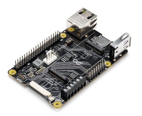
ASX00049

Arduino

* $43.33 - * $50.43

IN STOCK 2835
Buy

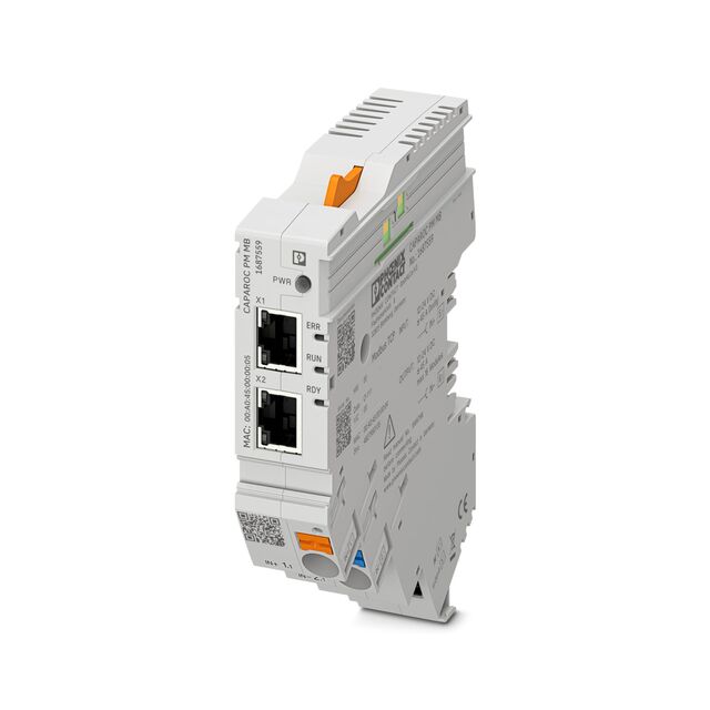
1687559

Phoenix Contact Ltd

[no prices available]

IN STOCK 4
Buy

Reference Designs

RD006

Wurth Elektronik

RD006 - 3 W Dual-output isolated auxiliary supply for communication interfaces and measurement systems

CN0583

Analog Devices Inc.

Multistandard Micropower Verified Smoke Detection System-on-Module

Technical Resources

EVALUATION KITS

EVAL-AD7124-8SDZ

Analog Devices Inc.

$0.00 - * $79.23

IN STOCK 792
Buy
View All