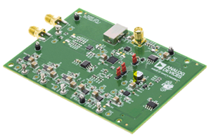
EV1HMC220BMS8G
Analog Devices Inc.The HMC220B is an ultraminiature, double-balanced mixer in an 8-lead mini small outline package with exposed pad (MINI_SO_EP). This fundamental, monolithic microwave integrated circuit (MMIC) mixer is constructed of gallium arsenide (GaAs) Schottky diodes and planar transformer baluns on the chip.The device can be used as an upconverter, downconverter, biphase demodulator, or phase comparator from 5 GHz to 12 GHz. The HMC220B provides excellent local oscillator (LO) to radio frequency (RF) and LO to intermediate frequency (IF) isolation due to optimized balun structures and operates as low as 7 dBm. The RoHS compliant HMC220B eliminates the need for wire bonding and is compatible with high volume surface-mount manufacturing techniques.Applications Very small aperture terminals (VSAT) and mobile satellite communication terminals Microwave and military radio Wireless backhaul equipment Automotive, dedicated short range communications (DSRC) and intelligent vehicle highway systems (IVHS) Military radar, electronic warfare (EW), and electronic counter measure (ECM) subsystems
EV1HMC241AQS16
Analog Devices Inc.The HMC241AQS16 & HMC241AQS16E are general purpose low-cost non-reflective SP4T switches in 16-lead QSOP packages. Covering DC - 3.5 GHz, this switch offers high isolation and has a low insertion loss of 0.7 dB at 2 GHz. The switch offers a single positive bias and true TTL/CMOS compatibility. A 2:4 decoder is integrated on the switch requiring only 2 control lines and a positive bias to select each path, replacing 8 control lines normally required by GaAs SP4T switches.APPLICATIONS Base Stations & Portable Wireless CATV/DBS Wireless Local Loop Test Equipment
EV1HMC329ALC3B
Analog Devices Inc.The HMC329ALC3B is a general-purpose, double balanced mixer in a leadless, RoHS compliant, surface-mount technology (SMT) package that can be used as an upconverter or down-converter between 24 GHz and 32 GHz. This mixer is fabricated in a gallium arsenide (GaAs), monolithic microwave integrated circuit (MMIC) process and requires no external components or matching circuitry. The HMC329ALC3B provides excellent local oscillator (LO) to radio frequency (RF) and LO to intermediate frequency (IF) suppression due to optimized balun preliminary structures. The mixer operates with LO amplitude above 9 dBm. The RoHS compliant HMC329ALC3B eliminates the need for wire bonding, allowing the use of surface-mount manufacturing techniques.Applications Microwave and very small aperture terminal (VSAT) radios Test equipment Military electronic warfare (EW) Electronic countermeasure (ECM) Command, control, communications, and intelligence (C3I)
EV1HMC4069LP4
Analog Devices Inc.The HMC4069LP4E is an Integer-N synthesizer which incorporates a 10 to 1300MHz digital phase-frequency detectorwith a 10 to 2900MHz 5-bit frequency counter. It is intended for use in low phase noise synthesizer applications.The combination of high frequency of operation along with its ultra low phase noise floor make possible synthesizerswith wide loop bandwidth and low N resulting in fast switching and very low phase noise. When used in conjunctionwith a differential loop amplifier, the HMC4069LP4E generates output voltages that can be used to phase lock a VCOto a reference oscillator.The device is packaged in a 24-pin, 4 x 4mm leadless QFN surface mount package with an exposed ground paddlefor improved RF and thermal performance.Applications Point-to-point radios Satellite communication systems Military applications Sonet clock generation
EV1HMC425ALP3E
Analog Devices Inc.HMC425ALP3E are broadband 6-bit GaAs IC digital attenuators in low cost leadless surfacemount packages. Covering 2.2 GHz to 8.0 GHz, the insertion loss is less than 4.5 dB typical. Theattenuator bit values are 0.5 (LSB), 1, 2, 4, 8, and 16 dB for a total attenuation of 31.5 dB. Attenuationaccuracy is excellent at ? 0.5 dB typical step error with an IIP3 of +40 dBm. Six control voltage inputs,toggled between 0 and +3 to +5V, are used to select each attenuation state. A single VDD bias of +3 to+5V is required.Applications WLAN & Point-to-Multi-Point Fiber Optics & Broadband Telecom Microwave Radio & VSAT Military
EV1HMC470ALP3
Analog Devices Inc.The HMC470A is a 5-bit digital attenuator with a 31 dBattenuation control range in 1 dB steps.The HMC470A offers excellent attenuation accuracy and high input linearity over the specified frequency range from 100 MHz to 3 GHz. However, this digital attenuator features ACG pins forexternal ac grounding capacitors to extend the operation below 100 MHz.The HMC470A operates with a single positive supply voltagefrom 3 V to 5 V and provides CMOS-/TTL-compatible parallelcontrol interface by incorporating an on-chip driver. TheHMC470A comes in a RoHS compliant, compact, 3 mm ? 3 mmLFCSP package.Applications Cellular infrastructure Microwave radios and very small aperture terminals (VSATs) Test equipment and sensors IF and RF designs
EV1HMC521ALC4
Analog Devices Inc.The HMC521ALC4 is a compact, gallium arsenide (GaAs), monolithic microwave integrated circuit (MMIC), inphase quadrature (I/Q) mixer in a RoHS compliant, 24-terminal ceramic leadless chip carrier (LCC) package. This device can be used as either an image reject mixer or a single sideband upconverter. The mixer uses two standard, double balanced mixer cells and a 90? hybrid coupler fabricated in a GaAs, metal?semiconductor field effect transistor (MESFET) process. This?device is a smaller alternative to hybrid style image reject?mixers and single sideband upconverter assemblies. The HMC521ALC4 eliminates the need for wire bonding, allowing?use of surface-mount manufacturing techniques.Applications Microwave and very small aperture terminal (VSAT) radios Test equipment Military electronic warfare (EW); electronic countermeasure (ECM); and command, control, communications, and intelligence (C3I)
EV1HMC629ALP4E
Analog Devices Inc.The HMC629ALP4E is a broadband 4-bit GaAs ICDigital Attenuator in a low cost leadless SMT package.This versatile digital attenuator incorporates off-chipAC ground capacitors for near DC operation, makingit suitable for a wide variety of RF and IF applications.The dual mode control interface is CMOS/TTL compatible,and accepts either a three wire serial input ora 4-bit parallel word. The HMC629ALP4E is housedin a RoHS compliant 4x4 mm QFN leadless package,and requires no external matching components.Applications Cellular/3G infrastructure WiBro / WiMAX / 4G Microwave radio & VSAT Test equipment and sensors? IF & RF applications
EV1HMC6787ALC5A
Analog Devices Inc.The HMC6787ALC5A is a compact GaAs MMIC I/Q variable gain upconverter in a leadless RoHS compliant SMT package. This device provides a small signal conversion gain of 11 dB with 17 dBc of sideband rejection, and 13 dB of gain control. The HMC6787ALC5A utilizes a RF variable gain amplifier preceded by an I/Q mixer where the LO is driven by a X2 multiplier. IF1 and IF2 mixer inputs are provided and an external 90? hybrid is needed to select the required sideband. The I/Q mixer topology reduces the need for filtering of the unwanted sideband. The HMC6787ALC5A is a much smaller alternative to hybrid style single sideband upconverter assemblies and it eliminates the need for wire bonding by allowing the use of surface mount manufacturing techniques.APPLICATIONS Point-to-Point and Point-to-Multi-Point Radio Military Radar, EW & ELINT Satellite Communications Sensors
EV1HMC6789BLC5A
Analog Devices Inc.The HMC6789BLC5A is a compact GaAs MMIC I/Qdownconverter in a 12-terminal, RoHS compliant,ceramic leadless chip carrier (LCC) package. Thisdevice provides a small signal conversion gain of 14 dBwith 25 dBc of image rejection. The HMC6789BLC5Autilizes a low noise amplifier to drive the I/Q mixerwhere the LO is driven by a ?2 multiplier. IF1 and IF2mixer inputs are provided and an external 90? hybridis needed to select the required sideband. The I/Qmixer topology reduces the need for filtering of theunwanted sideband. The HMC6789BLC5A is a muchsmaller alternative to hybrid style single sidebanddownconverter assemblies and it eliminates the needfor wire bonding by allowing the use of surface mountmanufacturing techniques.Applications Point-to-Point and Point-to-Multi-Point Radios Military Radar, EW & ELINT Satellite Communications Sensors
EV1HMC6832ALP5L
Analog Devices Inc.The HMC6832 is an input selectable, 2:8 differential fanoutbuffer designed for low noise clock distribution. The IN_SELcontrol pin selects one of the two differential inputs. This inputis then buffered to all eight differential outputs. The low jitteroutputs of the HMC6832 lead to synchronized low noiseswitching of downstream circuits, such as mixers, analog-todigitalconverters (ADCs)/digital-to-analog converters (DACs),or serializer/deserializer (SERDES) devices. The device is capableof low voltage, positive emitter-coupled logic (LVPECL) or lowvoltage differential signaling (LVDS) configurations by pullingthe CONFIG pin low for LVPECL or high or open (internallypulled high) for pseudo LVDS.Product Highlights Multiple Output Configurations. The CONFIG pin allows the user to select LVPECL or LVDS output termination. Multiple Supply Voltage Operation. The HMC6832 operates at 2.5 V or 3.3 V for LVPECL terminations (2.5 V only for LVDS). Low Noise. The HMC6832 noise is low, typically from ?168 dBc/Hz to ?162 dBc/Hz up to 3000 MHz. Low Propagation Delay. The HMC6832 displays a low delay, less than 207 ps, typical. Channel skew is also low, ?5 ps, typical. Low Core Current. The HMC6832 has a low core current of 56 mA, typical. Applications SONET, Fibre Channel, GigE clock distribution ADC/DAC clock distribution Low skew and jitter clocks Wireless/wired communications Level translation High performance instrumentation Medical imaging Single-ended to differential conversions
EV1HMC788ALP2
Analog Devices Inc.The HMC788A is a 0.01 GHz to 10 GHz, gain block, monolithic microwave integrated circuit (MMIC) amplifier using gallium arsenide (GaAs), pseudomorphic high electron mobility transistor (pHEMT) technology.This 2 mm ? 2 mm LFCSP amplifier can be used as either a cascadable 50 ? gain stage, or to drive the local oscillator (LO) port of many of the single and double balanced mixers from Analog Devices, Inc. with up to 20 dBm output power.The HMC788A offers 14 dB of gain and an output IP3 of 33 dBm while requiring only 76 mA from a 5 V supply.The Darlington feedback pair exhibits reduced sensitivity to normal process variations and yields excellent gain stability over temperature while requiring a minimal number of external bias components.Applications Cellular, 3G, LTE, WiMAX, and 4G LO driver applications Microwave radio Test and measurement equipment Ultra wideband (UWB) communications
EV1HMC7911LP5
Analog Devices Inc.The HMC7911 is a compact gallium arsenide (GaAs), pseudomorphic(pHEMT), monolithic microwave integrated circuit(MMIC) upconverter in a RoHS compliant, low stress, injectionmolded plastic LFCSP package that operates from 17 GHz to20 GHz. This device provides a small signal conversion gain of18 dB with 30 dBc of sideband rejection. The HMC7911 uses avariable gain amplifier preceded by an in-phase/quadrature (I/Q)mixer that is driven by an active 2? local oscillator (LO) multiplier.IF1 and IF2 mixer inputs are provided, and an external 90? hybridis needed to select the required sideband. The I/Q mixer topologyreduces the need for filtering of the unwanted sideband. TheHMC7911 is a much smaller alternative to hybrid style singlesideband (SSB) upconverter assemblies, and it eliminates theneed for wire bonding by allowing the use of surface-mountmanufacturing techniques.Applications Point to point and point to multipoint radios Military radars, electronic warfare (EW), and electronic intelligence (ELINT) Satellite communications Sensors
EV1HMC7912LP5
Analog Devices Inc.The HMC7912 is a compact, gallium arsenide (GaAs), pseudomorphic(pHEMT), monolithic microwave integrated circuit(MMIC) upconverter in a RoHS compliant, low stress, injectionmolded plastic LFCSP package that operates from 21 GHz to24 GHz. This device provides a small signal conversion gain of15 dB with 22 dBc of sideband rejection. The HMC7912 uses avariable gain amplifier preceded by an in-phase/quadrature (I/Q)mixer that is driven by an active 2? LO multiplier. IF1 and IF2mixer inputs are provided, and an external 90? hybrid is needed toselect the required sideband. The I/Q mixer topology reducesthe need for filtering of the unwanted sideband. The HMC7912is a much smaller alternative to hybrid style single sideband (SSB)upconverter assemblies, and it eliminates the need for wirebonding by allowing the use of surface-mount manufacturingtechniques.Applications Point to point and point to multipoint radios Military radars, electronic warfare (EW), and electronic intelligence (ELINT) Satellite communications Sensors
EV1HMC8073LP3D
Analog Devices Inc.The HMC8073 is a 6-bit digital step attenuator (DSA), operating from 0.6 GHz to 3.0 GHz, that features 31.5 dB of attenuation range with 0.5 dB steps.The HMC8073 is implemented in a silicon process, offering a fast settling time, low power consumption, and high electrostatic discharge (ESD) robustness. The device features safe state transitions, allowing attenuation state changes without overshooting, and is optimized for excellent step accuracy and high power and high linearity over frequency and temperature range. The radio frequency (RF) input and output are internally matched to 50 ? and do not require any external matching components. The design is bidirectional, and the RF input and output are interchangeable.The external address feature of the HMC8073 allows users to control up to eight DSAs using a single bus. The DSA has an on-chip regulator that supports a wide supply operating range from 3.3 V to 5.0 V with no performance change in electrical characteristics. The HMC8073 incorporates a complementary metal-oxide semiconductor (CMOS)- and transistor transitory logic (TTL)- compatible interface that supports serial (3-wire) control of the attenuator.The HMC8073 comes in an RoHS compliant, compact, 3 mm ? 3 mm LFCSP package.Applications Cellular infrastructure Microwave radios? Very small aperture terminals Test equipment and sensors
EV1HMC8412LP2F
Analog Devices Inc.The HMC8412 is a gallium arsenide (GaAs), monolithic microwave integrated circuit (MMIC), pseudomorphic high electron mobility transistor (pHEMT), low noise wideband amplifier that operates from 0.4 GHz to 11 GHz. The HMC8412 provides a typical gain of 15.5 dB, a 1.4 dB typical noise figure, and a typical output third-order intercept (OIP3) of ?33 dBm, requiring only 60 mA from a 5 V drain supply voltage. The saturated output power (PSAT) of ?20.5 dBm typical enables the low noise amplifier (LNA) to function as a local oscillator (LO) driver for many Analog Devices, Inc., balanced, inphase and quadrature (I/Q) or image rejection mixers. The HMC8412 also features inputs and outputs that are internally matched to 50 ?, making the device ideal for surface-mount technology (SMT)-based, high capacity microwave radio applications. The HMC8412 is housed in an RoHS-compliant, 2 mm ? 2 mm, 6-lead LFCSP.APPLICATIONS Test instrumentation Telecommunications Military radar and communication Electronic warfare Aerospace
EV1HMC936ALP6
Analog Devices Inc.The HMC936ALP6E is a 6-bit digital phase shifterwhich is rated from 1.2 to 1.4 GHz, providing 360degrees of phase coverage, with a LSB of 5.625degrees. The HMC936ALP6E features very low RMSphase error of 1.2 degrees and extremely low inser-tionloss variation of ?0.5 dB across all phase states. Thishigh accuracy phase shifter is controlled with positivecontrol logic of 0/+5V and requires no negative supplyvoltage. The HMC936ALP6E is housed in a compact6x6 mm plastic leadless SMT package and is internallymatched to 50 Ohms with no external components.Applications EW receivers? Weather and military radar Satellite communications Beamforming modules Phase cancellation
EV-21564L-SOM
Analog Devices Inc.Reaching speeds of up to 1 GHz, the ADSP-2159x processors are members of the SHARC? family of products. The ADSP-2159x processor is a dual-SHARC+? core DSP that doubles the audio performance of its single-SHARC+ core ADSP-2156x predecessor while maintaining pin-compatibility to it in the BGA package, providing design scalability from 400 MHz (ADSP-21566) to 2 GHz (ADSP-21593).The ADSP-2159x SHARC processors are members of the SIMD SHARC family of digital signal processors (DSPs) that feature Analog Devices, Inc., Super Harvard Architecture. These 32-bit/40-bit/64-bit floating-point processors are optimized for high performance audio/floating-point applications with large on-chip static random-access memory (SRAM), multiple internal buses that eliminate input/output (I/O) bottlenecks, and innovative digital audio interfaces (DAI). New additions to the SHARC+ core include cache enhancements and branch prediction, while maintaining instruction set compatibility to previous SHARC products.By integrating a rich set of industry-leading system peripherals and memory (see Table 1 in the data sheet), the SHARC+ processor is the platform of choice for applications that require programmability similar to reduced instruction set computing (RISC), multimedia support, and leading edge signal processing in one integrated package. These applications span a wide array of markets, including automotive, professional audio, and industrial-based applications that require high floating-point performance.APPLICATIONS Automotive: audio amplifier, head unit, ANC/RNC, rear seat entertainment, digital cockpit, ADAS Consumer & Professional Audio: speakers, sound bars, AVRs, conferencing systems, mixing consoles, microphone arrays, headphones
EV-AD5544/45SDZ
Analog Devices Inc.The AD5544/AD5554 quad, 16-/14-bit, current output, digital-to-analog converters (DACs) are designed to operate from 2.7 V to 5.5 V supply range.The applied external reference input voltage (VREFX) determines the full-scale output current. Integrated feedback resistors (RFB) provide temperature-tracking, full-scale voltage outputs when combined with an external I-to-V precision amplifier.A double-buffered serial data interface offers high speed, 3-wire, SPI- and microcontroller-compatible inputs using serial data in (SDI), a chip select (CS), and clock (CLK) signals. In addition, a serial data out pin (SDO) allows for daisy-chaining when multiple packages are used. A common, level-sensitive, load DAC strobe (LDAC) input allows the simultaneous update of all DAC outputs from previously loaded input registers. Additionally, an internal power-on reset forces the output voltage to 0 at system turn-on. An MSB pin allows system reset assertion (RS) to force all registers to zero code when MSB = 0, or to half-scale code when MSB = 1.The AD5544 is packaged in the compact 28-lead SSOP and 32-lead LFCSP. ?The AD5554 is ?packaged in the compact 28-lead SSOP.Applications Automatic test equipment Instrumentation Digitally controlled calibration
EV-ADF4001SD1Z
Analog Devices Inc.The ADF4001 frequency synthesizer can be used to implement clock sources for PLLs that require very low noise, stable reference signals. It consists of a low-noise digital PFD (Phase Frequency Detector), a precision charge pump, a programmable reference divider, and a programmable 13-bit N counter. In addition, the 14-bit reference counter (R Counter), allows selectable REFIN frequencies at the PFD input. A complete PLL (Phase-Locked Loop) can be implemented if the synthesizer is used with an external loop filter and VCO (Voltage Controlled Oscillator) or VCXO (Voltage Controlled Crystal Oscillator). The N min value of 1 allows flexibility in clock generation.?


