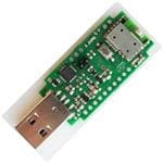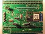

STEVAL-MKI134V1
STMicroelectronicsSTEVAL-MKI134V1- 3 Axis Sensor Adapter Board for Standard DIL 24 Socket
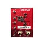
ISL28414TSSOPEVAL1Z
IntersilEvaluation Board For Single, Dual, Quad General Purpose Micropower, RRIO Operational Amplifiers
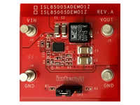
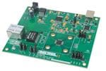
ISL85005ADEMO1Z
IntersilThe ISL85005DEMO1Z and ISL85005ADEMO1Z platforms allow quick demonstration of the high performance features of the ISL85005 and ISL85005A buck regulators.
The ISL85005 and ISL85005A are 4.5V to 18V input, 5A synchronous buck regulators for applications with input voltage from multi-cell batteries or regulated 5V and 12V power rails. These devices also provide an integrated bootstrap diode for the high-side gate driver to reduce the external parts count.
The ISL850xx sync buck regulators support input voltages of 3.8V to 18V and wide output current range, offering designers a complete portfolio of devices with high efficiency and reliable performance.
Features:
Switch selectable EN (enabled/disabled)
Selectable mode (DEM/Forced CCM) (ISL85005DEMO1Z)
Internal and external compensation options
Frequency synchronization option (ISL85005DEMO1Z)
Adjustable soft-start option (ISL85005ADEMO1Z)
Small and compact design
Applications:
Network and communication equipments
Battery powered systems
Multifunction printers
Point-of-load regulators
Standard 12V rail supplies
Embedded computing systems