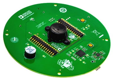
LTC4353DE Demo Board | Dual Low Voltage Ideal Diode Controller
Analog Devices Inc.DC1926A: Demo Board for the LTC4353 Dual Low Voltage Ideal Diode Controller.
DC1928A
Analog Devices Inc.The LTC3867 is a current mode synchronous step-down switching regulator controller that drives all N-channel power MOSFET stages. Output voltage transient excursions are minimized by use of a nonlinear control architecture to eliminate clock latency issues.The maximum current sense voltage is programmable from 30mV to 75mV, allowing the use of either a discrete sense resistor or the inductor DCR as the sensing element. Programmable DCR temperature compensation allows constant current limit regardless of inductor temperature. Programmable inductor temperature-based thermal shutdown protects the power components from thermal stress. Soft recovery from output shorts or overcurrent minimizes output overshoot.The LTC3867 features a precision 0.6V reference and can regulate output voltages up to 14V from a wide 4V to 38V input supply range. The LTC3867 includes a high speed differential remote sense amplifier. Burst Mode? operation, continuous and pulse-skipping modes are supported. The LTC3867 is available in a 24-lead (4mm ? 4mm) QFN package.Applications Automotive Systems Telecom Systems Industrial Equipment Distributed DC Power Systems
LTC3891EUDC Demo Board: 16V to 60V Input, VOUT = 12V at 15A
Analog Devices Inc.Demonstration circuit 1940A is a low quiescent current, synchronous buck converter featuring the LTC3891EUDC. This demo board converts a 16V to 60V voltage to a 12V at 15A output. The main features of this board include an internal LDO for gate drive power from VIN or EXTVCC, RUN and PGOOD pins, a mode selector that allows the converter to run in constant current mode (CCM), pulse-skipping or Burst Mode® operation, and selectable current limit. The DC1940A supports an adjustable output voltage, soft-start and tracking. The wide input voltage range of 16V to 60V is suitable for double battery automotive and distributed DC power systems where low quiescent current is important.
DC1942C
Analog Devices Inc.The LTC6804 is a 3rd generation multicell battery stack monitor that measures up to 12 series connected battery cells with a total measurement error of less than 1.2mV. The cell measurement range of 0V to 5V makes the LTC6804 suitable for most battery chemistries. All 12 cell voltages can be captured in 290?s, and lower data acquisition rates can be selected for high noise reduction.Multiple LTC6804 devices can be connected in series, permitting simultaneous cell monitoring of long, high voltage battery strings. Each LTC6804 has an isoSPI interface for high speed, RF-immune, local area communications. Using the LTC6804-1, multiple devices are connected in a daisy-chain with one host processor connection for all devices. Using the LTC6804-2, multiple devices are connected in parallel to the host processor, with each device individually addressed.Additional features include passive balancing for each cell, an onboard 5V regulator, and 5 general purpose I/O lines. In sleep mode, current consumption is reduced to 4?A. The LTC6804 can be powered directly from the battery, or from an isolated supply.Applications Electric and Hybrid Electric Vehicles Backup Battery Systems Grid Energy Storage High Power Portable Equipment
DC1954A-C
Analog Devices Inc.The LTC6954 is a family of very low phase noise clock distribution parts. Each part has three outputs and each output has an individually programmable frequency divider and delay. There are four members of the family, differing in their output logic signal type:LTC6954-1: Three LVPECL outputsLTC6954-2: Two LVPECL and one LVDS/CMOS outputsLTC6954-3: One LVPECL and two LVDS/CMOS outputsLTC6954-4: Three LVDS/CMOS outputsEach output is individually programmable to divide the input frequency by any integer from 1 to 63, and to delay each output by 0 to 63 input clock cycles. The output duty cycle is always 50%, regardless of the divide number. The LVDS/CMOS outputs are jumper selectable via the OUTxSEL pins to provide either an LVDS logic output or a CMOS logic output.The LTC6954 also features Linear Technology?s EZSync system for perfect clock synchronization and alignment every time.All device settings are controlled through an SPI-compatible serial port.Applications Clocking High Speed, High Resolution ADCs, DACs?and Data Acquisition Systems Low Jitter Clock Distribution
DC1959A-C
Analog Devices Inc.The LTC6948 is a high performance, low noise, 6.39GHz phase-locked loop (PLL) with a fully integrated VCO, including a reference divider, phase-frequency detector (PFD), ultralow noise charge pump, fractional feedback divider, and VCO output divider.The fractional divider uses an advanced, 4th order ?? modulator which provides exceptionally low spurious levels. This allows wide loop bandwidths, producing extremely low integrated phase noise values.The programmable VCO output divider, with a range of 1 through 6, extends the output frequency range.Applications Wireless Basestations (LTE, WiMAX, W-CDMA, PCS) Microwave Data Links Military and Secure Radio Test and Measurement
DC1964A
Analog Devices Inc.The LTC3110 is a 2A bidirectional buck-boost DC/DC regulator with capacitor charger and balancer. Its wide 0.1V to 5.5V capacitor/battery voltage and 1.8V to 5.25V system backup voltage ranges make it well suited to a wide variety of backup applications using supercapacitors or batteries. A proprietary low noise switching algorithm optimizes efficiency with capacitor/battery voltages that are above, below or equal to the system output voltage.The LTC3110 can autonomously transition from charge to backup mode or switch modes based on an external command. Pin-selectable Burst Mode operation reduces standby current and improves light-load efficiency, which combined with a 1?A shutdown current make the LTC3110 ideally suited for backup applications. Additional features include voltage supervisors for direction control and end of charge, and a general purpose comparator with open-collector output for interfacing with a ?C. The LTC3110 is available in thermally enhanced, low profile 24-lead TSSOP and 4mm ? 4mm QFN packages.Applications Supercapacitor Backup Converter and Charger Battery Backup Converter and Charger Servers, RAID Systems RF Systems with Battery/Capacitor Backup
DC196A-A
Analog Devices Inc.The LTC1543 is a 3-driver/3-receiver multiprotocol transceiver that operates from a single 5V supply. The LTC1543 and LTC1544 form the core of a complete software-selectable DTE or DCE interface port that supports the RS232, RS449, EIA530, EIA530-A, V.35, V.36 or X.21 protocols. Cable termination may be implemented using the LTC1344A software-selectable cable termination chip or by using existing discrete designs.The LTC1543 runs from a single 5V supply using an internal charge pump that requires only five space-saving surface mounted capacitors. The part is available in a 28-lead SSOP surface mount package.Applications Data Networking CSU and DSU Data Routers
LTC2974 Demo Board Kit (Includes DC1809 + DC1810), Requires DC1613
Analog Devices Inc.DC1978A: Demo Board for the LTC2974 4-Channel PMBus Power System Manager Featuring Accurate Output Current Measurement.
LTC5510 | Demo Board - (High Frequency) Input Frequency Range 30MHz to 3GHz; Output Range 1.2GHz to 2.1GHz
Analog Devices Inc.DC1983A: Demo Board for the LTC5510 1MHz to 6GHz Wideband High Linearity Active Mixer.
DC1984A
Analog Devices Inc.The LTC5510 is a high linearity mixer optimized for applications requiring very wide input bandwidth, low distortion, and low LO leakage. The chip includes a double-balanced active mixer with an input buffer and a high speed LO amplifier. The input is optimized for use with 1:1 transmission line baluns, allowing very wideband impedance matching. The mixer can be used for both up- and down-conversion and can be used in wideband systems.The LO can be driven differentially or single-ended and requires only 0dBm of LO power to achieve excellent distortion and noise performance, while also reducing external drive circuit requirements. The LTC5510 offers low LO leakage, greatly reducing the need for output filtering to meet LO suppression requirements.The LTC5510 is optimized for 5V but can also be used with a 3.3V supply with slightly reduced performance. The shutdown function allows the part to be disabled for further power savings.Applications Wideband Receivers/Transmitters Cable Downlink Infrastructure HF/VHF/UHF Mixer Wireless Infrastructure
DC1988A
Analog Devices Inc.The LTM8058 is a 2kV AC isolated flyback ?Module? (power module) DC/DC converter with LDO post regulator. Included in the package are the switching controller, power switches, transformer, LDO, and all support components. Operating over an input voltage range of 3.1V to 31V, the LTM8058 supports an output voltage range of 2.5V to 13V, set by a single resistor. There is also a linear post regulator whose output voltage is adjustable from 1.2V to 12V as set by a single resistor. Only output and input capacitors are needed to finish the design. Other components may be used to control the soft-start control and biasing.The LTM8058 is packaged in a thermally enhanced, compact (9mm ? 11.25mm ? 4.92mm) overmolded ball grid array (BGA) package suitable for automated assembly by standard surface mount equipment. The LTM8058 is available with SnPb or RoHS compliant terminal finish.Applications Industrial Sensors Industrial Switches Ground Loop Mitigation
LTM4676A Demo Board | LTM4676A(x2) Current Shared, PMBus Buck µModule, 4.5V ≤ VIN ≤ 17V, VOUT = 0.5V to 4V @ 50A
Analog Devices Inc.Demonstration circuit 1989B-A is a high efficiency, high density, μModule regulator with 4.5V to 17V input range. The output voltage is adjustable from 0.5V to 4V, and it can supply 50A maximum load current. The demo board has two LTM4676A μModule regulators, and the LTM4676A is a dual 13A or single 26A step-down regulator with PMBus power system management. Please see LTM4676A data sheet for more detailed information.
LTM4676A Demo Board | LTM4676A(x4) Current Shared, PMBus Buck µModule, 4.5V ≤ VIN ≤ 17V, VOUT = 0.5V to 4V @ 100A
Analog Devices Inc.Demonstration circuit 1989B-C is a high efficiency, high density, μModule regulator with 4.5V to 17V input range. The output voltage is adjustable from 0.5V to 4V, and it can supply 100A maximum load current. The demo board has four LTM4676A μModule regulators. The LTM4676A is a dual 13A or single 26A step-down regulator with PMBus power system management. Please see LTM4676A data sheet for more detailed information.
AD9645-125EBZ
Analog Devices Inc.The AD9645 is a dual, 14-bit, 80 MSPS/125 MSPS analog-to-digital converter (ADC) with an on-chip sample-and-hold circuit designed for low cost, low power, small size, and ease of use. The product operates at a conversion rate of up to 125 MSPS and is optimized for outstanding dynamic performance and low power in applications where a small package size is critical.The ADC requires a single 1.8 V power supply and LVPECL-/ CMOS-/LVDS-compatible sample rate clock for full performanceoperation. No external reference or driver components arerequired for many applications. The ADC automatically multiplies the sample rate clock for theappropriate LVDS serial data rate. A data clock output (DCO) for capturing data on the output and a frame clock output (FCO) forsignaling a new output byte are provided. Individual channelpower-down is supported; the AD9645 typically consumes lessthan 2 mW in the full power-down state. The ADC providesseveral features designed to maximize flexibility and minimize system cost, such as programmable output clock and data alignment and digital test pattern generation. The available digital test patterns include built-in deterministic and pseudorandom patterns, along with custom user-defined test patterns entered via the serial port interface (SPI). The AD9645 is available in a RoHS-compliant, 32-lead LFCSP. It is specified over the industrial temperature range of ?40?C to +85?C. This product is protected by a U.S. patent.PRODUCT HIGHLIGHTS Small Footprint. Two ADCs are contained in a small, spacesaving package. Low Power. The AD9645 uses 122 mW/channel at 125 MSPS with scalable power options. Pin Compatibility with the AD9635, a 12-Bit Dual ADC. Ease of Use. A data clock output (DCO) operates at frequencies of up to 500 MHz and supports double data rate (DDR) operation. User Flexibility. The SPI control offers a wide range of flexible features to meet specific system requirements.APPLICATIONS Communications Diversity radio systems Multimode digital receivers GSM, EDGE, W-CDMA, LTE, CDMA2000, WiMAX, TD-SCDMA I/Q demodulation systems Smart antenna systems Broadband data applications Battery-powered instruments Hand held scope meters Portable medical imaging and ultrasound Radar/LIDAR
AD9695-625EBZ
Analog Devices Inc.The AD9695 is a dual, 14-bit, 1300 MSPS/625 MSPS analog-to-digital converter (ADC). The device has an on-chip buffer and a sample-and-hold circuit designed for low power, small size, and ease of use. This product is designed to support communications applications capable of direct sampling wide bandwidth analog signals of up to 2 GHz. The ?3 dB bandwidth of the ADC input is 2 GHz. The AD9695 is optimized for wide input bandwidth, high sampling rate, excellent linearity, and low power in a small package.The dual ADC cores feature a multistage, differential pipelined architecture with integrated output error correction logic. Each ADC features wide bandwidth inputs supporting a variety of user-selectable input ranges. An integrated voltage reference eases design considerations. The analog input and clock signals are differential inputs. The ADC data outputs are internally connected to four digital downconverters (DDCs) through a crossbar mux. Each DDC consists of multiple signal processing stages: a 48-bit frequency translator (numerically controlled oscillator (NCO)), and decimation filters. The NCO has the option to select up to 16 preset bands over the general-purpose input/output (GPIO) pins, or use a coherent fast frequency hopping mechanism for band selection. Operation of the AD9695 between the DDC modes is selectable via SPI-programmable profiles.In addition to the DDC blocks, the AD9695 has several functions that simplify the automatic gain control (AGC) function in a communications receiver. The programmable threshold detector allows monitoring of the incoming signal power using the fast detect control bits in Register 0x0245 of the ADC. If the input signal level exceeds the programmable threshold, the fast detect indicator goes high. Because this threshold indicator has low latency, the user can quickly turn down the system gain to avoid an overrange condition at the ADC input. In addition to the fast detect outputs, the AD9695 also offers signal monitoring capability. The signal monitoring block provides additional information about the signal being digitized by the ADC.The user can configure the Subclasss 1 JESD204B-based high speed serialized output using either one lane, two lanes, or four lanes, depending on the DDC configuration and the acceptable lane rate of the receiving logic device. Multidevice synchronization is supported through the SYSREF? and SYNCINB? input pins.The AD9695 has flexible power-down options that allow significant power savings when desired. All of these features can be programmed using a 3-wire serial port interface (SPI) and or PDWN/STBY pin.The AD9695 is available in a Pb-free, 64-lead LFCSP and is specified over the ?40?C to +105?C junction temperature range. This product may be protected by one or more U.S. or international patents.Note that, throughout this data sheet, multifunction pins, such as FD_A/GPIO_A0, are referred to either by the entire pin name or by a single function of the pin, for example, FD_A, when only that function is relevant.Product Highlights Low power consumption per channel. JESD204B lane rate support up to 16 Gbps. Wide, full power bandwidth supports intermediate frequency (IF) sampling of signals up to 2 GHz. Buffered inputs ease filter design and implementation. Four integrated wideband decimation filters and NCO blocks supporting multiband receivers. Programmable fast overrange detection. On-chip temperature diode for system thermal management.Applications Communications Diversity multiband, multimode digital receivers 3G/4G, TD-SCDMA, WCDMA, GSM, LTE General-purpose software radios Ultrawideband satellite receiver Instrumentation Oscilloscopes Spectrum analyzers Network analyzers Integrated RF test solutions Radars Electronic support measures, electronic counter measures, and electronic counter-counter measures High speed data acquisition systems DOCSIS 3.0 CMTS upstream receive paths Hybrid fiber coaxial digital reverse path receivers Wideband digital predistortion
AD9706-DPG2-EBZ
Analog Devices Inc.The AD9704/AD9705/AD9706/AD9707 are the fourth-generation family in the TxDAC series of high performance, CMOS digital-to-analog converters (DACs). This pin-compatible, 8-/10-/12-/14-bit resolution family is optimized for low power operation, while maintaining excellent dynamic performance. The AD9704/AD9705/AD9706/AD9707 family is pin-compatible with the AD9748/AD9740/AD9742/AD9744 family of TxDAC converters and is specifically optimized for the transmit signal path of communication systems. All of the devices share the same interface, LFCSP package, and pinout, providing an upward or downward component selection path based on performance, resolution, and cost. The AD9704/AD9705/AD9706/AD9707 offers exceptional ac and dc performance, while supporting update rates up to 175 MSPS.The flexible power supply operating range of 1.7 V to 3.6 V and low power dissipation of the AD9704/AD9705/AD9706/AD9707 parts make them well suited for portable and low power applications.Power dissipation of the AD9704/AD9705/AD9706/AD9707 can be reduced to 15 mW, with a small trade-off in performance, by lowering the full-scale current output. In addition, a power-down mode reduces the standby power dissipation to approximately 2.2 mW.The AD9704/AD9705/AD9706/AD9707 has an optional serial peripheral interface (SPI?) that provides a higher level of programmability to enhance performance of the DAC. An adjustable output, common-mode feature allows for easy interfacing to other components that require common modes from 0 V to 1.2 V.Edge-triggered input latches and a 1.0 V temperature-compensated band gap reference have been integrated to provide a complete, monolithic DAC solution. The digital inputs support 1.8 V and 3.3 V CMOS logic families.PRODUCT HIGHLIGHTS Pin Compatible. The AD9704/AD9705/AD9706/AD9707 line of TxDAC?converters is pin-compatible with theAD9748/AD9740/AD9742/AD9744 TxDAC line (LFCSP package). Low Power. Complete CMOS DAC operates on a single supply of 3.6 V down to 1.7 V, consuming 50 mW (3.3 V) and 12 mW (1.8 V). The DAC full-scale current can be reduced for lower power operation. Sleep and power-down modes are provided for low power idle periods. Self-Calibration. Self-calibration enables true 14-bit INL and DNL performance in the AD9707. Twos Complement/Binary Data Coding Support. Data input supports twos complement or straight binary data coding. Flexible Clock Input. A selectable high speed, single-ended,and differential CMOS clock input supports 175 MSPS conversion rate. Device Configuration. Device can be configured through pin strapping, and SPI control offers a higher level of programmability. Easy Interfacing to Other Components. Adjustable common-mode output allows for easy interfacing to other signal chain components that accept common-mode levels from 0 V to 1.2 V. On-Chip Voltage Reference. The AD9704/AD9705/AD9706/AD9707 include a 1.0 V temperature-compensated band gap voltage reference. Industry-Standard 32-Lead LFCSP Package.
AD9708-EBZ
Analog Devices Inc.The AD9708 is the 8-bit resolution member of the TxDAC? series of high performance, low power CMOS digital-to-analog converters (DACs). The TxDAC? family, which consists of pin compatible 8-, 10-, 12-, and 14-bit DACs, was specifically optimized for the transmit signal path of communication systems. All of the devices share the same interface options, small outline package and pinout, thus providing an upward or downward component selection path based on performance, resolution and cost. The AD9708 offers exceptional ac and dc performance while supporting update rates up to 125 MSPS.The AD9708's flexible single-supply operating range of 2.7 V to 5.5 V and low power dissipation are well suited for portable and low power applications. Its power dissipation can be further reduced to 45 mW, without a significant degradation in performance, by lowering the full-scale current output. In addition, a power-down mode reduces the standby power dissipation to approximately 20 mW.The AD9708 is manufactured on an advanced CMOS process. A segmented current source architecture is combined with a proprietary switching technique to reduce spurious components and enhance dynamic performance. Edge-triggered input latches and a temperature compensated bandgap reference have been integrated to provide a complete monolithic DAC solution. Flexible supply options support +3 V and +5 V CMOS logic families.The AD9708 is a current-output DAC with a nominal full-scale output current of 20 mA and > 100 k Ohms output impedance.Differential current outputs are provided to support single-ended or differential applications. The current outputs may be directly tied to an output resistor to provide two complementary, single-ended voltage outputs. The output voltage compliance range is 1.25 V.The AD9708 contains a 1.2 V on-chip reference and reference control amplifier, which allows the full-scale output current to be simply set by a single resistor. The AD9708 can be driven by a variety of external reference voltages. The AD9708's full-scale current can be adjusted over a 2 mA to 20 mA range without any degradation in dynamic performance. Thus, the AD9708 may operate at reduced power levels or be adjusted over a 20 dB range to provide additional gain ranging capabilities.The AD9708 is available in a 28-pin SOIC package. It is specified for operation over the industrial temperature range.
AD9735-DPG2-EBZ
Analog Devices Inc.The AD9736, AD9735, and AD9734 are high performance, high frequency DACs that provide sample rates of up to 1200 MSPS, permitting multicarrier generation up to their Nyquist frequency. The AD9736 is the 14-bit member of the family, while the AD9735 and the AD9734 are the 12-bit and 10-bit members, respectively. They include a serial peripheral interface (SPI) port that provides for programming of many internal parameters and enables readback of status registers.A reduced-specification LVDS interface is utilized to achieve the high sample rate. The output current can be programmed over a range of 8.66 mA to 31.66 mA. The AD973x family is manufactured on a 0.18 ?m CMOS process and operates from 1.8 V and 3.3 V supplies for a total power consumption of 380 mW in bypass mode. It is supplied in a 160-lead chip scale ball grid array for reduced package parasitics.Product Highlights Low noise and intermodulation distortion (IMD) features enable high quality synthesis of wideband signals at intermediate frequencies up to 600 MHz. Double data rate (DDR) LVDS data receivers support the maximum conversion rate of 1200 MSPS. Direct pin programmability of basic functions or SPI port access offers complete control of all AD973x family functions. Manufactured on a CMOS process, the AD973x family uses a proprietary switching technique that enhances dynamic performance. The current output(s) of the AD9736 family are easily configured for single-ended or differential circuit topologies.Applications Broadband communications systems Cellular infrastructure (digital predistortion) Point-to-point wireless CMTS/VOD Instrumentation, automatic test equipment Radar, avionics
AD9736-DPG2-EBZ
Analog Devices Inc.The AD9736, AD9735, and AD9734 are high performance, high frequency DACs that provide sample rates of up to 1200 MSPS, permitting multicarrier generation up to their Nyquist frequency. The AD9736 is the 14-bit member of the family, while the AD9735 and the AD9734 are the 12-bit and 10-bit members, respectively. They include a serial peripheral interface (SPI) port that provides for programming of many internal parameters and enables readback of status registers.A reduced-specification LVDS interface is utilized to achieve the high sample rate. The output current can be programmed over a range of 8.66 mA to 31.66 mA. The AD973x family is manufactured on a 0.18 ?m CMOS process and operates from 1.8 V and 3.3 V supplies for a total power consumption of 380 mW in bypass mode. It is supplied in a 160-lead chip scale ball grid array for reduced package parasitics.Product Highlights Low noise and intermodulation distortion (IMD) features enable high quality synthesis of wideband signals at intermediate frequencies up to 600 MHz. Double data rate (DDR) LVDS data receivers support the maximum conversion rate of 1200 MSPS. Direct pin programmability of basic functions or SPI port access offers complete control of all AD973x family functions. Manufactured on a CMOS process, the AD973x family uses a proprietary switching technique that enhances dynamic performance. The current output(s) of the AD9736 family are easily configured for single-ended or differential circuit topologies.Applications Broadband communications systems Cellular infrastructure(digital predistortion) Point-to-point wireless CMTS/VOD Instrumentation, automatic test equipment Radar, avionics


