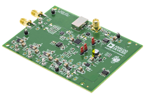
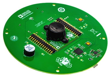
DC1054A with DC1054B | LTC4242 Dual PCI Express Hot Swap Controller
Analog Devices Inc.DC1054A/B: Demo Board for the LTC4242 Dual Slot Hot Swap Controller for PCI Express.

LTC3219EUD Demo Board | 9-Channel Charge Pump LED Driver, 2.9V ≤ VIN ≤ 5.5V, VLED = up to 5V @ 28mA per LED (DC590 Requires)
Analog Devices Inc.Demonstration circuit 1055 is a 250mA Universal Nine Channel Multimode (1x, 1.5x, 2x) Charge Pump LED Driver with two RGB displays and three white LEDs featuring the LTC3219. The LTC3219 is a low noise charge pump designed to drive nine universal LED current sources. The input voltage range is 2.9V to 5.5V. Each channel provides 28mA of LED current.
The LTC3219 requires only five small ceramic capacitors to form a complete LED power supply and current controller. The maximum display currents are set with an internal precision current reference. On/Off blinking, gradation, and intensity are achieved via an I2C serial interface. There are 64 dimming states available for the universal LEDs. The DC590 controller board is required for proper operation.

LTC3520EUF| Buck-Boost with 400mA Buck, VIN = 2.2V to 5.5V, VOUT1 = 3.3V @ 1A (BB), VOUT2 = 1.8V @ 0.6A, VOUT3 (LDO Post Regulator) = 1.5V @ 200mA
Analog Devices Inc.Demonstration circuit 1062 is a micropower synchronous buck-boost + buck converter based on the LTC3520. The DC1062 has an input voltage range of 2.2V to 5.5V and three output voltages: 3.3V @ up to 1A, 1.8V @ 600mA and 1.5V @ 200mA. The 1.5VOUT is an LDO regulator derived from either the 3.3VOUT or the 1.8VOUT.

LTC4355 Demoboard | Positive High Voltage Ideal Diode-OR
Analog Devices Inc.DC1066A: Demo Board for the LTC4355 Positive High Voltage Ideal Diode-OR with Input Supply and Fuse Monitors.

LTC2450-1 | 16-bit 60Hz ΔΣ ADC in 2 × 2 DFN (Requires DC590B)
Analog Devices Inc.DC1067A-B: Demo Board for the LTC2450-1 Easy-to-Use, Ultra-Tiny 16-Bit ΔΣ ADC.

DC1079A-A
Analog Devices Inc.The LTC4310 provides bidirectional I2C communications between two I2C buses whose grounds are isolated from one another. Each LTC4310 encodes I2C bus logic states into signals that are transmitted across an isolation barrier to another LTC4310. The receiving LTC4310 decodes the transmission and drives its l2C bus to the appropriate logic state. The isolation barrier can be bridged by an inexpensive Ethernet, or other transformer, to achieve communications across voltage differences reaching thousands of volts, or it can be bridged by capacitors for lower voltage isolation. The LTC4310-1 is intended for use in 100kHz I2C systems. The LTC4310-2 is intended for 400kHz I2C systems.Rise time accelerators provide strong pull-up currents on SCL and SDA rising edges to meet rise time specifications for heavily loaded systems. Data and clock Hot Swap? circuitry prevent data corruption when a card is inserted into or removed from a live bus. When a bus is stuck low for 37ms, the LTC4310 turns off its pull-down devices and generates up to sixteen clocks and a STOP bit in an attempt to free the bus. Driving EN low sets the LTC4310 in a very low current shutdown mode to conserve power.Applications Isolated I2C, SMBus and PMBus Interfaces Isolated Power Supplies Positive-to-Negative Rail Communications Power-over-Ethernet

LTC2954 | Push Button On/Off Controller with uP Interrupt
Analog Devices Inc.DC1090A: Demo Board for LTC2954 Push Button On/Off Controller with µP Interrupt

LT3570EUF Demo Board | Buck + Boost + LDO Controller, 4V to 36VIN Buck with VOUT1 = 3.3V@1A, 3.3V to 10VIN Boost with VOUT2 = 12V@275mA, 100mA LDO
Analog Devices Inc.Demonstration circuit 1106 is a 1.5A Buck Converter, 1.5A Boost Converter, and LDO Controller featuring the LT3570. The Buck is designed to convert a 4V to 36V source to 3.3V at 1A. The LDO is powered from the output of the buck and converts 3.3V to 2.5V at 100mA. The boost converts a 3.3V to 10V source to 12V at 275mA.

LT6411 650MHz Different ADC Driver
Analog Devices Inc.DC1108A - Demo Board for:LT6411 - 650MHz Differential ADC Driver/Dual Selectable Gain Amplifier
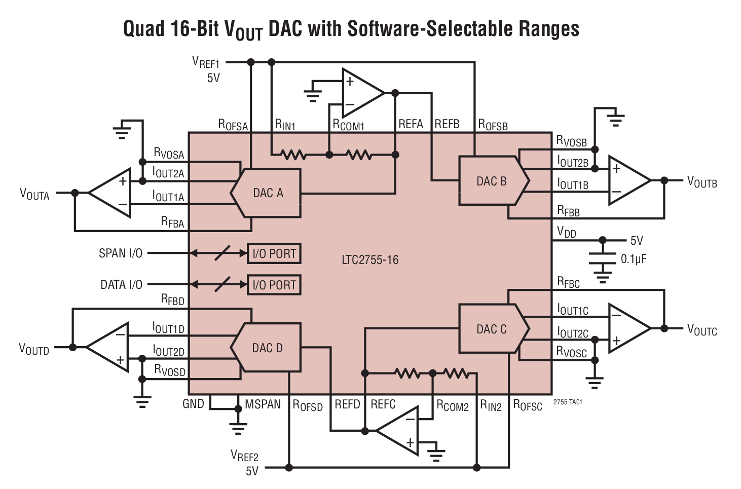
LTC2755: 16-bit, Quad, SoftSpan, 1LSB INL IOUT DAC, requires DC590
Analog Devices Inc.DC1112A: Demo Board for LTC2755-16 Quad Current Output 16-Bit SoftSpan DACs with Parallel I/O

LTC6102 Current Sense Demo Board
Analog Devices Inc.DC1113A: Demo Board for the LTC6102 Precision Zero Drift Current Sense Amplifier

LTC3850EUF Demo Board | 6.5V ≤ VIN ≤ 14V, VOUT = 3.3V @ 5A & 2.5V @ 5A
Analog Devices Inc.Demonstration circuit 1126 is a high density dual output (3.3V/5A and 2.5V/5A) step down converter featuring the LTC3850EUF. The input voltage range is 6.5V to 14V. For applications that have a 5V +/- 0.5V input, the board has an optional resistor to tie the INTVCC pin to the VIN pin.
An optional DCR sense circuit allows the converter to use the inductors DCR as the sense element instead of the on-board sense resistors to save cost and board space and to improve efficiency.

LTC3419EDD Demo Board | 2.25MHz, 2.5V ≤ VIN ≤ 5.5V, VOUT1 = 1.2V/1.5V/1.8V @ 600mA, VOUT2 = 2.5V/3.3V @ 600mA
Analog Devices Inc.Demonstration circuit 1128A is a dual channel synchronous, 2.25MHz Step-Down DC/DC Regulator featuring the LTC3419. The DC1128A has an input voltage range of 2.5V to 5.5V. Both jumper selectable 3.3V/2.5V and 1.2V/1.5V/1.8V outputs are capable of delivering up to 600mA of output current. The device also features independent internal soft-start for each channel.

LTC2242CUP-12 | CMOS OUT, VCC = 2.5V, 250Msps, 12-Bit, 10MHz < AIN < 250MHz, Need DC890
Analog Devices Inc.DC1133A-A: Demo Board for the LTC2242-12 12-Bit, 250Msps ADC.

LTC6403-1 Demo Circuit
Analog Devices Inc.DC1147A-E: Demo Board for the LTC6403-1 200MHz, Low Noise, Low Power Fully Differential Input/Output Amplifier/Driver

LTC3873ETS8 Isolated/Non-Isolated Demo Board | 36 ≤ VIN ≤ 72V, VOUT: 3.3V/3A
Analog Devices Inc.Demonstration circuit DC1154 is a Telecom non isolated DC/DC converter featuring the LTC3873 constant frequency current mode flyback controller. The DC1154 converts 36V to 72V input voltage to an isolated 3A of output current at 3.3V. The 200kHz constant frequency operation is maintained down to very light load to reduce low frequency noise generated over a wide range of load current. The DC1154 also provides an isolated design by installing the optocoupler and LTC4430 related circuitry. The demonstration circuit can be easily modified to generate different output voltages up to 15V. As output voltage is increased, the maximum output current must be reduced to limit the output power to no more than 10W.

LTC3565EDD Demo Board | 1.25A, 4MHz, Synchronous Step-Down DC/DC Converter
Analog Devices Inc.DC1159A: Demo Board for LTC3565 1.25A, 4MHz, Synchronous Step-Down DC/DC Converter

LTC3725EMSE/LTC3726EGN 1/8 Brick | 9V < VIN < 36V, VOUT: 15V/3A
Analog Devices Inc.DC1174A-C: Demo Board for the LTC3725 Single-Switch Forward Controller and Gate Driver and LTC3726 Secondary-Side Synchronous Forward Controller

LTC3522EUD Demo Board | Buck-Boost Plus Buck, 2.4V ≤ VIN ≤ 4.3V, VOUT1 = 3.3V @ 300mA, VOUT2 = 1.8V @ 200mA
Analog Devices Inc.Demonstration circuit DC1177 is a micropower dual Buck-Boost/Buck synchronous converter based on the LTC3522 monolithic regulator. The DC1177 has an input voltage range of 2.4V to 4.2V and outputs 3.3V @ 300mA and 1.8V @ 200mA.

LTC2361 Demo Board | 12-Bit, 250ksps SAR ADC (Requires DC590B for DC Apps, DC890B for AC Apps)
Analog Devices Inc.DC1190A-D: Demo Board for the LTC2361 250ksps, 12-Bit Serial ADCs in TSOT-23