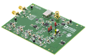
ADRF6650-EVALZ
Analog Devices Inc.The ADRF6650 is a highly integrated downconverter that integrates dual mixers, dual digital switched attenuators, dual digital variable gain amplifiers, a phase-locked loop (PLL), and voltage controlled oscillators (VCOs). In addition, the ADRF6650 integrates two radio frequency (RF) baluns, serial gain control (SGC) controls, and fast enable inputs for time division duplex (TDD) operation.The on-chip RF baluns enable the ADRF6650 to support 50 ? terminated RF inputs. The integrated passive mixer provides a highly linear downconversion for a 200 MHz, sliding, intermediate frequency (IF) window. The ADRF6650 uses broadband square wave limiting local oscillator (LO) amplifiers to achieve an RF bandwidth of 450 MHz to 2700 MHz. Unlike conventional narrow-band sine wave LO amplifier solutions, this amplifier permits the LO to be applied either above or below the RF input over an extremely wide bandwidth.The ADRF6650 offers two alternatives for generating the differential LO input signal: internally via the on-chip fractional-N synthesizer with low phase noise VCOs, or externally via a low phase noise LO signal. The integrated PLL/VCO enables continuous LO coverage from 450 MHz to 2900 MHz. The PLL referenceinput supports a wide frequency range and includes integrated reference dividers before the phase frequency detector (PFD).The ADRF6650 is fabricated using an advanced silicon-germanium (SiGe) bipolar complementary metal-oxide semiconductor(BiCMOS) process. It is available in a 56-lead, RoHS-compliant, 8 mm ? 8 mm, lead frame chip scale package (LFCSP) package with an exposed pad. Performance is specified over the ?40?C to +105?C maximum paddle temperature.Applications Multiband/multistandard cellular base station diversity receivers Wideband radio link diversity downconverters Multimode cellular extenders and picocells

ADRF6780-EVALZ
Analog Devices Inc.The ADRF6780 is a silicon germanium (SiGe) design, wideband,microwave upconverter optimized for point to point microwaveradio designs operating in the 5.9 GHz to 23.6 GHz frequencyrange.The upconverter offers two modes of frequency translation. The device is capable of direct conversion to radio frequency (RF) from baseband I/Q input signals, as well as single sideband (SSB) upconversion from a real intermediate frequency (IF) input carrier frequency. The baseband inputs are high impedance and are generally terminated off chip with 100 ? differential back terminations. The baseband I/Q input path can be disabled and a modulated real IF signal anywhere from 0.8 GHz to 3.5 GHz can fed into the IF input path and upconverted to 5.9 GHz to 23.6 GHz while suppressing the unwanted sideband by typically better than 25 dBc. The serial port interface (SPI) allows tweaking of the quadrature phase adjustment to allow optimum sideband suppression. In addition, the SPI interface allows powering down the output power detector to reduce power consumption when power monitoring is not necessary.The ADRF6780 upconverter comes in a compact, thermallyenhanced, 5 mm ? 5 mm LFCSP package. The ADRF6780operates over the ?40?C to +85?C temperature range.APPLICATIONS Point to point microwave radios Radar, electronic warfare systems Instrumentation, automatic test equipment (ATE)

ADRV9002NP/W1/PCBZ
Analog Devices Inc.The ADRV9002 is a highly integrated RF transceiver that has dual-channel transmitters, dual-channel receivers, integrated synthesizers, and digital signal processing functions.The ADRV9002 is a high performance, highly linear, high dynamic range transceiver designed for performance vs. power consumption system optimization. The device is configurable and ideally suited to demanding, low power, portable and battery powered equipment. The ADRV9002 operates from 30 MHz to 6000 MHz and covers the UHF, VHF, industrial, scientific, and medical (ISM) bands, and cellular frequency bands in narrow-band (kHz) and wideband operation up to 40 MHz. The ADRV9002 is capable of both TDD and FDD operation.The transceiver consists of direct conversion signal paths with state-of-the-art noise figure and linearity. Each complete receiver and transmitter subsystem includes dc offset correction, quadrature error correction (QEC), and programmable digital filters, which eliminate the need for these functions in the digital baseband. In addition, several auxiliary functions, such as auxiliary analog-to-digital converters (ADCs), auxiliary digital-to-analog converters (DACs), and general-purpose inputs/outputs (GPIOs), are integrated to provide additional monitoring and control capability.The fully integrated phase-locked loops (PLLs) provide high performance, low power, fractional-N frequency synthesis for the transmitter, receiver, and clock sections. Careful design and layout techniques provide the isolation required in high performance personal radio applications. All voltage controlled oscillator (VCO) and loop filter components are integrated to minimize the external component count. The local oscillators (LOs) have flexible configuration options and include fast lock modes.The transceiver includes low power sleep and monitor modes to save power and extend the battery life of portable devices while monitoring communications.The fully integrated, low power digital predistortion (DPD) is optimized for both narrow-band and wideband signals and enables linearization of high efficiency power amplifiers.The ADRV9002 core can be powered directly from 1.0 V, 1.3 V, and 1.8 V regulators and is controlled via a standard 4-wire serial port. Other voltage supplies are used to provide proper digital interface levels and to optimize the receiver, transmitter, and auxiliary converter performance.High data rate and low data rate interfaces are supported using configurable CMOS or low voltage differential signaling (LVDS) serial synchronous interface (SSI) choice.The ADRV9002 is packaged in a 12 mm ? 12 mm, 196-ball chip scale package ball grid array (CSP_BGA).APPLICATIONS Mission critical communications Very high frequency (VHF), ultrahigh frequency (UHF), and cellular to 6 GHz Time division duplexing (TDD) and frequency division duplexing (FDD) applications

ADRV9008-1W/PCBZ
Analog Devices Inc.The receive path consists of two independent, wide bandwidth (BW), direct conversion receivers with state-of-the-art dynamic range. The complete receive subsystem includes automatic and manual attenuation control, dc offset correction, quadrature error correction (QEC), and digital filtering, eliminating the need for these functions in the digital baseband. RF front-end control and several auxiliary functions such as analog-to-digital converters (ADCs), digital-to-analog converters (DACs), and general-purpose input/outputs (GPIOs) for the power amplifier (PA) are also integrated.In addition to automatic gain control (AGC), the ADRV9008-1 also features flexible external gain control modes, allowing significant flexibility in setting system level gain dynamically.The received signals are digitized with a set of four high dynamic range, continuous time, sigma-delta (?-?) ADCs that provide inherent antialiasing. The combination of the direct conversion architecture, which does not suffer from out of band image mixing, and the lack of aliasing relaxes the requirements of the RF filters compared to traditional intermediate frequency (IF) receivers.The fully integrated phase-locked loop (PLL) provides high per-formance, low power, fractional-N, RF synthesis for the receiver signal paths. An additional synthesizer generates the clocks needed for the converters, digital circuits, and the serial interface. A multi-chip synchronization mechanism synchronizes the phase of the RF local oscillator (LO) and baseband clocks between multiple ADRV9008-1 chips. Precautions are taken to provide the isolation required in high performance base station applications. All voltage controlled oscillators (VCOs) and loop filter components are integrated.The high speed JESD204B interface supports up to 12.288 Gbps lane rates, resulting in two lanes per transmitter and a single lane per receiver in the widest bandwidth mode. The interface also supports interleaved mode for lower bandwidths, reducing the total number of high speed data interface lanes to one. Both fixed and floating point data formats are supported. The floating point format allows internal AGC to be invisible to the demodulator device.The core of the ADRV9008-1 can be powered directly from 1.3 V and 1.8 V regulators and is controlled via a standard 4-wire serial port. Comprehensive power-down modes are included to mini-mize power consumption during normal use. The ADRV9008-1 is packaged in a 12 mm ? 12 mm, 196-ball chip scale ball grid array (CSP_BGA).Applications 3G, 4G, and 5G FDD, macrocell base stations Wide band active antenna systems Massive multiple input, multiple output (MIMO) Phased array radar Electronic warfare Military communications Portable test equipment
ADRV9026-LB/PCBZ
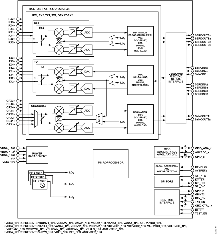
Analog Devices Inc.The ADRV9026 is a highly integrated, radio frequency (RF) agile transceiver offering four independently controlled transmitters, dedicated observation receiver inputs for monitoring each transmitter channel, four independently controlled receivers, integrated synthesizers, and digital signal processing functions providing a complete transceiver solution. The device provides the performance demanded by cellular infrastructure applications, such as small cell base station radios, macro 3G/4G/5G systems, and massive multiple in/multiple out (MIMO) base stations. The receiver subsystem consists of four independent, wide bandwidth, direct conversion receivers with wide dynamic range. The four independent transmitters use a direct conversion modulator resulting in low noise operation with low power consumption. The device also includes two wide bandwidth, time shared, observation path receivers with two inputs each for monitoring transmitter outputs. The complete transceiver subsystem includes automatic and manual attenuation control, dc offset correction, quadrature error correction (QEC), and digital filtering, eliminating the need for these functions in the digital baseband. Other auxiliary functions such as analog-to-digital converters (ADCs), digital-to-analog converters (DACs), and general-purpose input/outputs (GPIOs) that provide an array of digital control options are also integrated. To achieve a high level of RF performance, the transceiver includes five fully integrated phase-locked loops (PLLs). Two PLLs provide low noise and low power fractional-N RF synthesis for the transmitter and receiver signal paths. A third fully integrated PLL supports an independent local oscillator (LO) mode for the observation receiver. The fourth PLL generates the clocks needed for the converters and digital circuits, and a fifth PLL provides the clock for the serial data interface. A multichip synchronization mechanism synchronizes the phase of all LOs and baseband clocks between multiple ADRV9026 chips. All voltage controlled oscillators (VCOs) and loop filter components are integrated and adjustable through the digital control interface. The serial data interface consists of four serializer lanes and four deserializer lanes. The interface supports both the JESD204B and JESD204C standards, operating at data rates up to 24.33 Gbps. The interface also supports interleaved mode for lower bandwidths, thus reducing the number of high speed data interface lanes to one. Both fixed and floating-point data formats are supported. The floating-point format allows internal automatic gain control (AGC) to be invisible to the demodulator device. The ADRV9026 is powered directly from 1.0 V, 1.3 V, and 1.8 V regulators and is controlled via a standard serial peripheral interface (SPI) serial port. Comprehensive power-down modes are included to minimize power consumption in normal use. The ADRV9026 is packaged in a 14 mm ? 14 mm, 289-ball chip scale ball grid array (CSP_BGA).Applications 3G/4G/5G TDD and FDD massive MIMO, macro and small cell base stations

ADTR1107-EVALZ
Analog Devices Inc.The ADTR1107 is a compact, 6 GHz to 18 GHz, front-end IC?with an integrated power amplifier, low noise amplifier (LNA), and a reflective single-pole double-throw (SPDT) switch. These?integrated features make the device ideal for phased array antenna and radar applications. The front-end IC offers 25 dBm of saturated output power (PSAT) and 22?dB small signal gain in?transmit state, and 18 dB small signal gain and 2.5 dB noise figure in receive state. The device has a directional coupler for power detection. The input/outputs (I/Os) are internally matched to 50 ?. The ADTR1107 is supplied in a 5 mm ? 5 mm, 24-terminal, land grid array (LGA) package.Applications Phased array antenna Military radar Weather radar Communication links Electronic warfare

ADV3002-EVALZ
Analog Devices Inc.The ADV3002 is a complete HDMI?/DVI link switch featuring equalized transition minimized differential signaling (TMDS) inputs, ideal for systems with long cable runs. The ADV3002 includes bidirectional buffering for the DDC bus and CEC line, with integrated pull-up resistors for the CEC line. Additionally, the ADV3002 includes an EDID replication function that enables one EDID EEPROM to be shared for all four HDMI ports.The ADV3002 is provided in a space-saving, 80-lead LQFP surface-mount Pb-free plastic package and is specified to operate over the 0?C to 85?C temperature range.PRODUCT HIGHLIGHTS Input cable equalizer enables use of long cables at the input. For a 24 AWG cable, the ADV3002 compensates for more than 20m at data rates up to 3 Gbps. Auxiliary multiplexer isolates and buffers the DDC bus and the CEC line, increasing total system capacitance limit. EDID replication eliminates the need for multiple EDID EEPROMs. EDID can be loaded from a single external EEPROM or from a system microcontroller. 5 V power combiner powers the EDID replicator and CEC buffer when local system power is off. Integrated hot plug detect pulse low on channel switch with programmable pulse width or direct manual control.APPLICATIONS Advanced television (HDTV) sets Projectors A/V receivers Set-top boxes

ADV3219-EVALZ
Analog Devices Inc.The ADV3219 and ADV3220 are high speed, high slew rate,buffered, 2:1 analog multiplexers. They offer a ?3 dB signalbandwidth greater than 800 MHz and channel switch times ofless than 20 ns with 1% settling. With ?82 dB of crosstalk and?88 dB isolation (at 5 MHz), the ADV3219 and ADV3220 areuseful in many high speed applications. The differential gain ofless than 0.02% and the differential phase of less than 0.02?,together with 0.1 dB flatness beyond 100 MHz while driving a75 ? back terminated load, make the ADV3219 and ADV3220ideal for all types of signal switching. The ADV3219/ADV3220 include an output buffer that can beplaced into a high impedance state to allow multiple outputs tobe connected together for cascading stages without the off channelsloading the output bus. The ADV3219 has a gain of +1, and theADV3220 has a gain of +2; they both operate on ?5 V supplieswhile consuming less than 7.5 mA of idle current.The ADV3219/ADV3220 are available in the 8-lead LFCSPpackage over the extended industrial temperature range of?40?C to +85?C. Applications Routing of high speed signals including ??Video (NTSC, PAL, S, SECAM, YUV, and RGB) ??Compressed video (MPEG, wavelet) ??3-level digital video (HDB3) Data communications Telecommunications

ADV3221-EVALZ
Analog Devices Inc.The ADV3221 and?ADV3222 are high speed, high slew rate, buffered 4:1 analog multiplexers. They offer a ?3 dB signal bandwidth greater than 800 MHz and channel switch times of less than 20 ns with 1% settling. With lower than ?58 dB of crosstalk and ?67 dB isolation (at 100 MHz), the ADV3221 and ADV3222 are useful in many high speed applications. The diffe-rential gain error of less than 0.02% and differential phase error of less than 0.02?, together with 0.1 dB gain flatness out to 100 MHz while driving a 75 ? back terminated load, make the ADV3221 and ADV3222 ideal for all types of signal switching.The ADV3221/ADV3222 include an output buffer that can be placed into a high impedance state. This allows multiple outputs to be connected together for cascading stages without the off channels loading the output bus. The ADV3221 has a gain of +1, and the ADV3222 has a gain of +2; they both operate on ?5 V supplies while consuming less than 7.5 mA of idle current. The channel switching is performed via latched control lines, allowing synchronous updating in a multiple ADV3221/ADV3222 envi-ronment.The ADV3221/ADV3222 are offered in a 16-lead SOIC package and are available over the extended industrial temperature range of ?40?C to +85?C.Applications Routing of high speed signals including ? ? Video (NTSC, PAL, S, SECAM, YUV, RGB) ? ? Compressed video (MPEG, wavelet) ? ? 3-level digital video (HDB3) ? ? Data communications ? ? Telecommunications
ADV3222-EVALZ
Analog Devices Inc.The?ADV3221 ?and ADV3222 are high speed, high slew rate, buffered 4:1 analog multiplexers. They offer a ?3 dB signal bandwidth greater than 800 MHz and channel switch times of less than 20 ns with 1% settling. With lower than ?58 dB of crosstalk and ?67 dB isolation (at 100 MHz), the ADV3221 and ADV3222 are useful in many high speed applications. The differential gain error of less than 0.02% and differential phase error of less than 0.02?, together with 0.1 dB gain flatness out to 100 MHz while driving a 75 ? back terminated load, make the ADV3221 and ADV3222 ideal for all types of signal switching.The ADV3221/ADV3222 include an output buffer that can be placed into a high impedance state. This allows multiple outputs to be connected together for cascading stages without the off channels loading the output bus. The ADV3221 has a gain of +1, and the ADV3222 has a gain of +2; they both operate on ?5 V supplies while consuming less than 7.5 mA of idle current. The channel switching is performed via latched control lines, allowing synchronous updating in a multiple ADV3221/ADV3222 envi-ronment.The ADV3221/ADV3222 are offered in a 16-lead SOIC package and are available over the extended industrial temperature range of ?40?C to +85?C.Applications Routing of high speed signals including ? ? Video (NTSC, PAL, S, SECAM, YUV, RGB) ? ? Compressed video (MPEG, wavelet) ? ? 3-level digital video (HDB3) ? ? Data communications ? ? Telecommunications

ADV3225-EVALZ
Analog Devices Inc.The ADV3224/ADV3225 are high speed 16 ? 8 analog crosspoint switch matrices. They offer a ?3 dB signal bandwidth of greater than 750 MHz and a high slew rate of greater than 2500 V/?s.The ADV3224/ADV3225 include eight independent output buffers that can be placed into a high impedance state for paralleling crosspoint outputs to prevent off channels from loading the output bus. The ADV3224 has a gain of +1 and the ADV3225 has a gain of +2, and they both operate on voltage supplies of ?5 V. Channel switching is performed via a serial digital control that can accommodate the daisy chaining of several devices or via a parallel control to allow updating of an individual output without reprogramming the entire array.The ADV3224/ADV3225 are available in the 72-lead LFCSP package over the extended industrial temperature range of ?40?C to +85?C.ApplicationsRouting of high speed signals includingVideo (NTSC, PAL, S, SECAM, YUV, RGB)Compressed video (MPEG, wavelet)3-level digital video (HDB3)Data communicationsTelecommunications

ADV3226-EVALZ
Analog Devices Inc.The ADV3226/ADV3227 are high speed 16 ? 16 analog crosspoint switch matrices. They offer a ?3 dB signal bandwidth greater than 750 MHz and channel switch times of less than 20 ns with 1% settling.The ADV3226/ADV3227 include 16 independent output buffers that can be placed into a high impedance state for paralleling crosspoint outputs to prevent off channels from loading the output bus. The ADV3226 has a gain of +1 and the ADV3227 has a gain of +2. They both operate on voltage supplies of ?5 V while consuming only 118 mA (ADV3226) and 133 mA (ADV3227) of idle current. Channel switching is performed via a serial digital control that can accommodate daisy chaining of several devices or via a parallel control to allow updating of an individual output without reprogramming the entire array.The ADV3226/ADV3227 are available in the 100-lead LFCSP package over the extended industrial temperature range of ?40?C to +85?C.Applications Routing of high speed signals including ? ? Video (NTSC, PAL, S, SECAM, YUV, RGB) ? ? Compressed video (MPEG, wavelet) ? ? 3-level digital video (HDB3) Data communications Telecommunications

ADXL203EB
Analog Devices Inc.The ADXL203 is a high precision, low power, complete dual-axis accelerometer with signal conditioned voltage outputs, all on a single, monolithic IC. The ADXL203 measures acceleration with a full-scale range of ?1.7 g, ?5 g, or ?18 g. The ADXL203 can measure both dynamic acceleration (for example, vibration) and static acceleration (for example, gravity).The typical noise floor is 110 ?g/?Hz, allowing signals below 1 mg (0.06? of inclination) to be resolved in tilt sensing applications using narrow bandwidths (

ADXL204EB
Analog Devices Inc.The ADXL204 is a high precision, low power, complete dual-axis accelerometer with signal-conditioned voltage outputs, all on a single monolithic IC. Like the ADXL203, it measures acceleration with a full-scale range of ?1.7 g; however, the ADXL204 is tested and specified for 3.3 V supply voltage, whereas the ADXL203 is tested and specified at 5 V. Both parts function well over a wide 3 V to 6 V operating voltage range. The ADXL204 can measure both dynamic acceleration (for example, vibration) and static acceleration (for example, gravity).The typical noise floor is 170 ?g/?Hz, allowing signals below 2 mg (0.1? of inclination) to be resolved in tilt sensing applications using narrow bandwidths (

ADZS-A2B-ANALYZER
Analog Devices Inc.The Automotive Audio Bus? (A2B?) is an innovative technology that reduces system cost, weight, and design complexity by distributing audio and control data, together with clock and power over a single, low-cost, unshielded twisted pair cable. The AD2425W is an enhanced A2B transceiver offering an expanded feature set while retaining complete compatibility with existing AD241x devices. The AD2425W is fully configurable supporting both master and slave functionality.The AD2425W is targeted for use in wiring intensive applications where reducing the weight or complexity of existing cable harnesses is a primary system design objective. These applications include Premium Audio Systems, Active Noise Cancellation, and In-Car Communications.Applications Automotive audio communication link Active noise cancellation Microphone arrays for hands free and in car communication

DC043A
Analog Devices Inc.The LTC1286/LTC1298 are micropower, 12-bit, successive approximation sampling A/D converters. They typically draw only 250?A of supply current when converting and automatically power down to a typical supply current of 1nA whenever they are not performing conversions. They are packaged in 8-pin SO packages and operate on 5V to 9V supplies. These 12-bit, switched-capacitor, successive approximation ADCs include sample-and-holds. The LTC1286 has a single differential analog input. The LTC1298 offers a software selectable 2-channel MUX.On-chip serial ports allow efficient data transfer to a wide range of microprocessors and microcontrollers over three wires. This, coupled with micropower consumption, makes remote location possible and facilitates transmitting data through isolation barriers.These circuits can be used in ratiometric applications or with an external reference. The high impedance analog inputs and the ability to operate with reduced spans (to 1.5V full scale) allow direct connection to sensors and transducers in many applications, eliminating the need for gain stages.Applications Battery-Operated Systems Remote Data Acquisition Battery Monitoring Handheld Terminal Interface Temperature Measurement Isolated Data Acquisition

DC047A
Analog Devices Inc.The LTC1262 is a regulated 12V, 30mA output DC/DC converter. It is designed to provide the 12V ?5% output necessary to program byte-wide flash memories. The output will provide up to 30mA from input voltages as low as 4.75V without using any inductors. Only four external capacitors are required to complete an extremely small surface mountable circuit.The TTL compatible shutdown pin can be directly connected to a microprocessor and reduces the supply current to less than 0.5?A. The LTC1262 offers improved shutdown current performance and requires fewer external components than competing solutions.The LTC1262 is available in an 8-pin PDIP or SO-8 package.Applications 12V Flash Memory Programming Supplies Compact 12V Op Amp Supplies Battery-Powered Systems

DC088A
Analog Devices Inc.The LT1304 is a micropower step-up DC/DC converter ideal for use in small, low voltage, battery-operated systems. The devices operate from a wide input supply range of 1.5V to 8V. The LT1304-3.3 and LT1304-5 generate regulated outputs of 3.3V and 5V and the adjustable LT1304 can deliver output voltages up to 25V. Quiescent current, 120?A in active mode, decreases to just 10?A in shutdown with the low-battery detector still active. Peak switch current, internally set at 1A, can be reduced by adding a single resistor from the ILIM pin to ground. The high speed operation of the LT1304 allows the use of small, surface-mountable inductors and capacitors. The LT1304 is available in an 8-lead SO package.Applications 2-, 3-, or 4-Cell to 5V or 3.3V Step-Up Portable Instruments Bar Code Scanners Palmtop Computers Diagnostic Medical Instrumentation Personal Data Communicators/Computers

DC092A-A
Analog Devices Inc.The LTC1550/LTC1551 are switched capacitor charge pump voltage inverters which include internal linear post-regulators to minimize output ripple. Output voltages are fixed at ?4.1V, with ripple voltages typically below 1mVP-P. The LTC1550 is also available in an adjustable output voltage version. The LTC1550/LTC1551 are ideal for use as bias voltage generators for GaAs transmitter FETs in portable RF and cellular telephone applications. The LTC1550/LTC1551 operate from single 4.5V to 6.5V supplies and draw typical quiescent currents of 4.25mA with a 5V supply. Each device includes a TTL compatible Shutdown pin which drops supply current to 0.2?A typically. The LTC1550 Shutdown pin is active low (SHDN), while the LTC1551 Shutdown pin is active high (SHDN). Only four external components are required: an input bypass capacitor, two 0.1?F charge pump capacitors and a filter capacitor at the linear regulator output. The adjustable LTC1550 requires two additional resistors to set the output voltage. The LTC1550/LTC1551 will supply up to 10mA output current with a 5V supply, while maintaining guaranteed output regulation of ?5%. The fixed voltage LTC1550/LTC1551 are available in S0-8 plastic packages. The adjustable LTC1550 is available in a 16-pin SSOP.Applications GaAs FET Bias Generators Negative Supply Generators Battery-Powered Systems Single Supply Applications
DC092A-B
Analog Devices Inc.The LTC1550/LTC1551 are switched capacitor charge pump voltage inverters which include internal linear post-regulators to minimize output ripple. Output voltages are fixed at ?4.1V, with ripple voltages typically below 1mVP-P. The LTC1550 is also available in an adjustable output voltage version. The LTC1550/LTC1551 are ideal for use as bias voltage generators for GaAs transmitter FETs in portable RF and cellular telephone applications. The LTC1550/LTC1551 operate from single 4.5V to 6.5V supplies and draw typical quiescent currents of 4.25mA with a 5V supply. Each device includes a TTL compatible Shutdown pin which drops supply current to 0.2?A typically. The LTC1550 Shutdown pin is active low (SHDN), while the LTC1551 Shutdown pin is active high (SHDN). Only four external components are required: an input bypass capacitor, two 0.1?F charge pump capacitors and a filter capacitor at the linear regulator output. The adjustable LTC1550 requires two additional resistors to set the output voltage. The LTC1550/LTC1551 will supply up to 10mA output current with a 5V supply, while maintaining guaranteed output regulation of ?5%. The fixed voltage LTC1550/LTC1551 are available in S0-8 plastic packages. The adjustable LTC1550 is available in a 16-pin SSOP.Applications GaAs FET Bias Generators Negative Supply Generators Battery-Powered Systems Single Supply Applications