Receiver Skew Margin for Channel Link I and FPD Link I Devices
Texas InstrumentsCorrecting the Low-Frequency Response of the ADS42LBxx, ADS42JBxx for Time-Domai
Texas InstrumentsMethod of Graphing Safe Operating Area (SOA) Curves in DC-DC Converter
Texas InstrumentsReduce Electrical Stresses in a PFC stage during an AC drop test with UCD3138
Texas InstrumentsSupport Selfie Sticks Using a TS3A227E Audio Jack Switch
Texas InstrumentsGeneric Wrist Watch Programmer's Guide (Rev. A)
Texas InstrumentsGeneration of a VCOM buffer input using PWM signal
Texas InstrumentsPower Consumption Analysis for Low Power Capacitive Sensing Applications
Texas Instruments
Five Steps to a Good PCB Layout of the Boost Converter
Texas InstrumentsA good PCB layout is critical for the boost converter. The reason is that the boost converter is sensitive to parasitic capacitance and inductance because of the switch-mode operation. The bad PCB layout would introduce large parasitic capacitance and inductance, which would cause high output ripple, poor output voltage regulation and current limit accuracy, electromagnetic interference (EMI) problem, and even failure by the high voltage spike. Proper PCB layout will help to avoid most of these problems of the boost converter without extra cost if thought is spent before the first PCB is built.
Copying the layout of the boost converter from its datasheet or evaluation module (EVM) is easiest, but the layout may not fit the system board. So this application note details five steps that help to design a good PCB layout for the TPS61xxx converter.
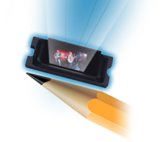
TI DLP® Pico™ System Design: Brightness Requirements and Tradeoffs
Texas InstrumentsThe objective of this application note is to help product developers who are new to DLP Pico technology understand brightness and the related system tradeoffs.


