

LTM8064IY#PBF
Part Number : LTM8064IY#PBF
Analog Devices Inc.Switching Voltage Regulators 58VIN, 6A CVCC Step-Down ?Module Regulator
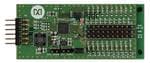
MAX11300PMB1#
Part Number : MAX11300PMB1#
Analog Devices Inc.Data Conversion IC Development Tools PMOD FOR MAX11300 12B, 20 PORT Configurable IO Device - TQFN Package
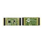
DS28E17K#
Part Number : DS28E17K#
Analog Devices Inc.Interface Development Tools EVALUATION KIT FOR DS28E17 (1W TO I2C BRDG)
LT3015MPQ#PBF
Part Number : LT3015MPQ#PBF
Analog Devices Inc.LDO Voltage Regulators 1.5A, L N, Neg Lin Reg w/ Prec C Lim
LTC1609ISW#PBF
Part Number : LTC1609ISW#PBF
Analog Devices Inc.Analog to Digital Converters - ADC 16-Bit, 200ksps, Serial Sampling ADC with Multiple Input Ranges
LTM8023MPY#PBF
Part Number : LTM8023MPY#PBF
Analog Devices Inc.Switching Voltage Regulators 2A, 36V DC/DC Step-Down ?Module (Power Module) Regulator
DS21354L
Part Number : DS21354L
Analog Devices Inc.Telecom Interface ICs 3.3/5V E1 Single Chip Transceiver
LTM8048MPY#PBF
Part Number : LTM8048MPY#PBF
Analog Devices Inc.Switching Voltage Regulators 3.1VIN to 32VIN Isolated ?Module (Power Module) DC/DC Converter with LDO Post Regulator
MAX4427EPA+
Part Number : MAX4427EPA+
Analog Devices Inc.Gate Drivers Dual High-Speed, 1.5A MOSFET Drivers

ICM7217AIPI
Part Number : ICM7217AIPI
Analog Devices Inc.LED Display Drivers 4-Digit Presettable LED Up/Down Counter
LTM4601AHVMPY#PBF
Part Number : LTM4601AHVMPY#PBF
Analog Devices Inc.Switching Voltage Regulators 12A, 28VIN DC/DC Module Regualtor with PLL, Output Tracking and Margining

MAX6865UK31D4S+T
Part Number : MAX6865UK31D4S+T
Analog Devices Inc.Supervisory Circuits Single nPower Supervisor


