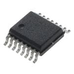

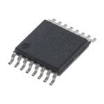
DS3152N+
Part Number : DS3152N+
Analog Devices Inc.Telecom Interface ICs Dual DS3/E3/STS-1 Line Interface Unit

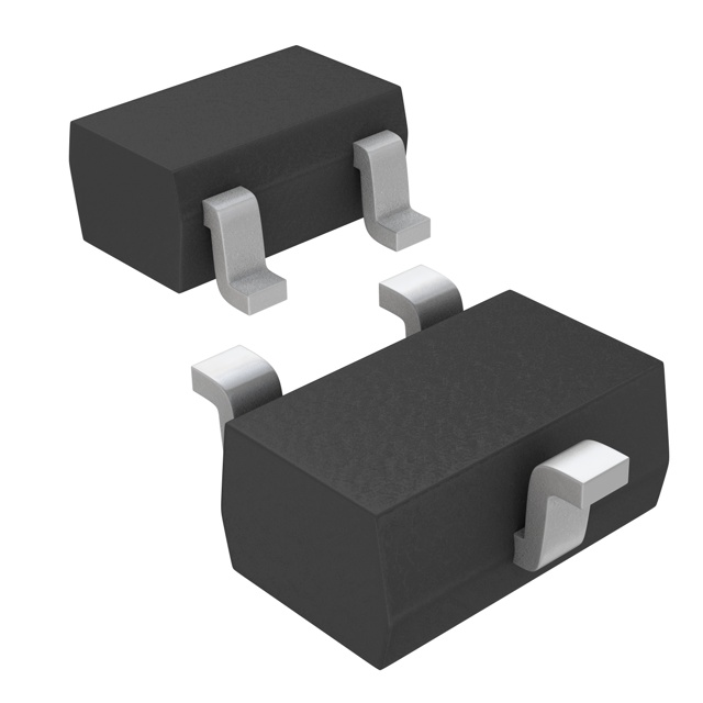
MAX9051AEUT-T
Part Number : MAX9051AEUT-T
Analog Devices Inc.Analog Comparators uPower Comparator + Prec Reference IC

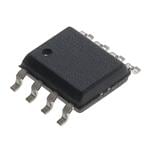
MAX700CPA
Part Number : MAX700CPA
Analog Devices Inc.Supervisor Push-Pull, Push-Pull 1 Channel 8-PDIP
MAX4662CAE+
Part Number : MAX4662CAE+
Analog Devices Inc.Analogue Switch ICs 2.5 Ohm Quad, SPST, CMOS Analog Switches


MAX6337US23D3-T
Part Number : MAX6337US23D3-T
Analog Devices Inc.Supervisor Open Drain or Open Collector 1 Channel SOT-143-4
MAX6381XR18D2-T
Part Number : MAX6381XR18D2-T
Analog Devices Inc.Supervisor Push-Pull, Totem Pole 1 Channel SC-70-3

MAX6368LKA29-T
Part Number : MAX6368LKA29-T
Analog Devices Inc.Supervisor Push-Pull, Totem Pole 1 Channel SOT-23-8
MAX8672EVKIT+
Part Number : MAX8672EVKIT+
Analog Devices Inc.Power Management IC Development Tools Eval Kit MAX8672 (Complete Backup Management IC for NiMH Batteries)

MAX4167ESA
Part Number : MAX4167ESA
Analog Devices Inc.General Purpose Amplifier 2 Circuit Rail-to-Rail 8-SOIC
MAX9107ESA+T
Part Number : MAX9107ESA+T
Analog Devices Inc.Analog Comparators 25ns, Dual/Quad/Single, Low-Power, TTL C

MAX6309UK46D3
Part Number : MAX6309UK46D3
Analog Devices Inc.Supervisor Push-Pull, Totem Pole 2 Channel SOT-23-5

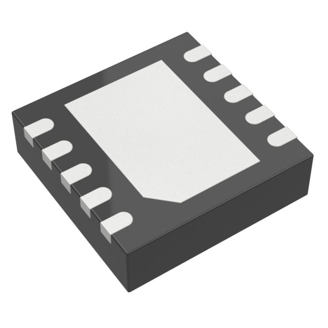
MAX20072ATAA/V
Part Number : MAX20072ATAA/V
Analog Devices Inc.Buck Switching Regulator IC Positive Adjustable 0.5V 1 Output 1A 8-WFDFN Exposed Pad


