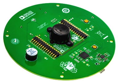
DC3080A-KIT
Analog Devices Inc.The LTC4126-ADJ is a low-power wireless single-cell Li-Ion battery charger with an integrated step-down DC/DC regulator. The step-down regulator is a low-noise multimode charge pump which is powered from the battery and provides a regulated 1.2V at the output. The switching frequency is set to either 50kHz or 75kHz depending on the mode to keep any switching noise out of the audible range.The constant-current constant-voltage Li-Ion battery charger has automatic recharge, automatic termination by safety timer, and battery temperature monitoring via an NTC pin. Charge current is programmable from 1mA to 50mA via an external resistor. Undervoltage protection disconnects the battery from all loads when the battery voltage is below 3.0V.The small package and minimal external component count make the LTC4126-ADJ and its variants suitable for hearing aid applications and other low power portable devices. See the chart in the data sheet.APPLICATIONSHearing AidsLow Power Li-Ion Powered DevicesWireless HeadsetsIoT Wearables
DC3082A-B
Analog Devices Inc.The LTM4681 is a quad 31.25A or single 125A stepdown??Module? (power module) DC/DC regulator featuring?remote configurability and telemetry-monitoring?of power management parameters over PMBus. The?LTM4681 is comprised of digitally programmable analog?control loops, precision mixed-signal circuitry, EEPROM,?power MOSFETs, inductors and supporting components.The LTM4681?s 2-wire serial interface allows outputs?to be margined, tuned and ramped up and down at programmable?slew rates with sequencing delay times. True input current sense, output currents and voltages, output?power, temperatures, uptime and peak values are readable. Custom configuration of the EEPROM contents is not?required. At start-up, output voltages, switching frequency,?and channel phase angle assignments can be set by pinstrapping?resistors. The LTpowerPlay? GUI and DC1613?USB-to-PMBus converter and demo kits are available.?The LTM4681 is offered in a 15mm ? 22mm ? 8.17mm?BGA package available with SnPb or RoHS compliant?terminal finish.APPLICATIONS Multi-Rail Processor Power, Configurable Core Power
LTM4681 Demo Board | PolyPhase Single Output Step-Down µModule Regulator with Digital PSM: 4 × LTM4681 at 480A
Analog Devices Inc.Demonstration circuit DC3082A-C features the LTM4681: the wide input and output voltage range, high efficiency and power density, high current PolyPhase® single output DC/DC step-down μModule® regulator with digital power system management. DC3082A-C is configured as 16-phase single output using 4× LTM4681. The factory default input voltage is 12V typical, output voltage is 1V at 480A typical or 500A peak with recommended 400LFM forced airflow. The demo board output voltages can be adjusted from 0.6V to 1V. Programming the output voltages to any value that is greater than 1V, requires derating output current based on thermal derating curves provided in the data sheet of the LTM4681. Heat sink or other appropriate electronic cooling systems can also be used in conjunction with forced airflow to further optimize the output power when the output is on and loaded with maximum output current. The factory default switching frequency is preset at 350kHz typical. DC3082A-C comes with PMBus interface and digital power system management functions. An onboard 12-pin connector is available for users to connect the dongle DC1613A to the demo board, provides an easy way to communicate and program the part using LTpowerPlay® software development tool. LTpowerPlay software and I2C/PMBus/SMBus dongle DC1613A allows users to monitor real time telemetry of input and output voltages, input and output current, switching frequency, internal IC die temperatures, power stage component temperatures and fault logs. Programmable parameters include device address, output voltages, control loop compensation, switching frequency, phase interleaving, DCM or CCM mode of operation, digital soft-start, sequencing and time based shutdown, fault responses to input and output overvoltage, output overcurrent, IC die and power component overtemperature.
The LTM4681 is available in a thermally enhanced, low profile 330-Lead (15mm × 22mm × 8.17mm) BGA package. It is recommended to read the data sheet and the demo manual of LTM4681 prior to use or making any hardware changes to DC3082A-C.
LTpowerPlay software can be downloaded here.
USB to PMBus Controller Dongle DC1613A for use with LTpowerPlay is available here.
LTC2980-24 | 24-Channel Power Supply System Featuring the LTC2980-24 Power System Manager
Analog Devices Inc.The DC3097A-KIT is a demonstration system for the LTC2980-24 for the 24-channel I2C/SMBus/PMBus Power System Manager (PSM) with EEPROM. It consists of 4 circuit boards, namely one DC3094A board and three DC1361B boards. The LTC2980-24 monitors and controls 24 power supply rails which are provided by three DC1361B power supply boards that plug into the DC3094A. The system demonstrates the ability of the LTC2980-24 to sequence, trim, margin, supervise, monitor, and log faults for the twenty-four power supplies. Together these four boards form a sophisticated, 24-channel, digitally programmable and digitally managed power supply system.
The board set contains twenty-four independent power supply rails, by having the three DC1361B boards. All 24 rails are based on LTM4603 DC/DC μModule® switching regulators. The DC1361B board is pre-configured with output voltages ranging from 0.8V to 3.3V. The power supply channels may be reconfigured to different output voltages by changing the feedback resistors. The LTC2980-24 can be configured to monitor current on odd numbered channels. The DC1361B board has been designed to allow the user to enable this feature on Channel 7. In this configuration, Channel 7 measures the current on Channel 6’s 1V output.
The LTpowerPlay® graphical user interface (GUI) supports this demonstration system and enables complete control of all the features of the LTC2980-24. Together, the LTpowerPlay software and DC3094A hardware system create a powerful development environment for designing and testing configuration settings of the LTC2980-24. LTpowerPlay stores these settings in the LTC2980-24 internal EEPROM or in a project file. The software displays all the configuration settings and real time measurements from the Power System Management IC. Telemetry allows easy access and decoding of the fault log created by the LTC2980-24. The board comes pre-programmed with the EEPROM values appropriate for the twenty-four power supply rails. Just plug and play!
Order preprogrammed devices from Analog Devices Express (ADX) using LTpowerPlay:
www.analog.com/programming
The DC3097A-KIT demo boards can be powered by an external power supply, such as a +12VDC supply. Communication with the software is provided through the DC1613 USB-to-I2C/SMBus/PMBus Controller. The following items are required:
+12VDC Power Supply
USB-to-I2C/SMBus/PMBus Controller (DC1613)
LTpowerPlay Software
DC3122A
Analog Devices Inc.The LTC3307A is a very small, high efficiency, low noise, monolithic synchronous 3A step-down DC/DC converter operating from a 2.25V to 5.5V input supply. Using constant frequency, peak current mode control at switching frequencies 1MHz to 3MHz and minimum on-time as low as 22ns, this regulator achieves fast transient response with small external components. Silent Switcher architecture minimizes EMI emissions.The LTC3307A operates in forced continuous or pulse skip mode for low noise, or low-ripple Burst Mode operation for high efficiency at light loads, ideal for battery-powered systems. The IC regulates output voltages as low as 500mV. Other features include output overvoltage protection, short-circuit protection, thermal shutdown, clock synchronization, and up to 100% duty cycle operation for low dropout. The device is available in a low profile 12-lead 2mm ? 2mm ? 0.74mm LQFN package with exposed pad for low thermal resistance.APPLICATIONS Optical Networking, Servers, Telecom Automotive, Industrial, Communications Distributed DC Power Systems (POL) FPGA, ASIC, ?P Core Supplies Battery Operated Systems
DC3129A-KIT
Analog Devices Inc.The LTC5597 is a high accuracy RMS power detector that provides a very wide RF input bandwidth, from 100MHz up to 70GHz. This makes the device suitable for a wide range of RF and microwave applications, such as point-to-point microwave links, instrumentation and power control applications. The DC output voltage of the detector is an accurate representation of the average signal power applied to the RF input. The response is linear-in-dB with 28.5mV/dB logarithmic slope over a 35dB dynamic range with typically better than ?1dB accuracy. The detector is particularly suited for measurement of waveforms with crest factor (CF) as high as 12dB, and waveforms that exhibit a significant variation of the crest factor during measurement. To achieve higher accuracy and lower output ripple, the averaging bandwidth can be externally adjusted by a capacitor connected between the FLTR and OUT pins. The enable interface switches the device between active measurement mode and a low power shutdown mode.Applications Point-to-Point Microwave Links SATCOM Instrumentation and Measurement Equipment Military Radios 5G, LTE, WiFi, Wireless Networks RMS Power Measurement Receive and Transmit Gain Control RF PA Transmit Power Control
LT8642-1 | 18V, 10A Synchronous Step-Down Silent Switcher
Analog Devices Inc.Demonstration circuit 3162A is a 18V, 10A synchronous step-down Silent Switcher® with spread spectrum frequency modulation featuring the LT8642-1. The demo board is designed for 1.2V output from a 2.8V to 18V input. The LT8642-1 is a compact, low emission, high efficiency, and high speed synchronous monolithic stepdown switching regulator. Special Silent Switcher architecture minimizes EMI emissions. Selectable spread spectrum mode can further improve EMI performance. Fast minimum on-time of 20ns enables high VIN to low VOUT conversion at high frequency.
The LT8642-1 switching frequency can be programmed either via a resistor or external clock over a 200kHz to 3MHz range. The default frequency of demo circuit 3162A is 2MHz. The LT8642-1 SYNC/MODE pin on the demo board is grounded (JP1 at BURST position) by default for low ripple Burst Mode® operation. Spread spectrum mode and forced continuous mode can be selected respectively by moving JP1 shunt. To synchronize to an external clock, move JP1 to FCM/SYNC and apply the external clock to the SYNC terminal.
The LT8642-1 data sheet gives a complete description of the part, operation, and application information. The data sheet must be read in conjunction with this demo manual for demo circuit 3162A. The LT8642-1 is assembled in a 3mm × 4mm LQFN package with exposed pads for low thermal resistance. The layout recommendations for low EMI operation and maximum thermal performance are available in the data sheet section Low EMI PCB Layout and Thermal Considerations.
LTC1751EMS8 | Regulated Charge Pump DC/DC Converter, 2.5V to 4.5V Input, 4VOUT @ 75mA
Analog Devices Inc.DC323A-C: Demo Board for LTC1751 Micropower, Regulated Charge Pump DC/DC Converters.
DC326C
Analog Devices Inc.The LT1766/LT1766-5 are 200kHz monolithic buck switching regulators that accept input voltages up to 60V. A high efficiency 1.5A, 0.2? switch is included on the die along with all the necessary oscillator, control and logic circuitry. A current mode control architecture delivers fast transient response and excellent loop stability.Special design techniques and a new high voltage process achieve high efficiency over a wide input range. Efficiency is maintained over a wide output current range by using the output to bias the circuitry and by utilizing a supply boost capacitor to saturate the power switch. Patented circuitry maintains peak switch current over the full duty cycle range. A shutdown pin reduces supply current to 25?A and the device can be externally synchronized from 228kHz to 700kHz with logic-level inputs.The LT1766/LT1766-5 are available in a 16-pin fused-lead SSOP package or a TSSOP package with exposed backside for improved thermal performance.Applications High Voltage, Industrial and Automotive Portable Computers Battery-Powered Systems Battery Chargers Distributed Power Systems
DC349B
Analog Devices Inc.The LTC1700 is a current mode synchronous step-up DC/DC controller that drives external N-channel and P-channel power MOSFETs using a constant frequency PWM architecture. Current limiting is provided by sensing the voltage drop across the main MOSFET, eliminating the need of a sense resistor. This No RSENSE? technique helps the LTC1700 maintain high efficiency at heavy loads while Burst Mode operation ensures high efficiency at light loads, thus providing high efficiencies over a wide range of load currents.The LTC1700 operates at a minimum input voltage as low as 0.9V. The device boasts a ?1.5% output voltage accuracy and consumes only 200?A of quiescent current. In shutdown, it only draws 10?A.To prevent inductor current runaway, the duty cycle is limited to 90%. Overvoltage protection is also provided which shuts both the external MOSFETs off when tripped.High constant operating frequency of 530kHz allows the use of small inductors and output capacitors. The LTC1700 can also be synchronized between 400kHz to 750kHz. Burst Mode operation is inhibited when the device is externally clocked or when the SYNC/MODE pin is pulled low to reduce noise and RF interference.Applications Cellular Telephones Wireless Modems RF Communications 2.5V to 3.3V, 2.5V to 5V Converters Battery-Powered Equipment Telecom/Network Systems
DC370A-B
Analog Devices Inc.The LTC1734 is a low cost, single cell, constant-current/constant-voltage Li-Ion battery charger controller. When combined with a few external components, the SOT-23 package forms a very small, low cost charger for single cell lithium-ion batteries.The LTC1734 is available in 4.1V and 4.2V versions with 1% accuracy. Constant current is programmed using a single external resistor between the PROG pin and ground. Manual shutdown is accomplished by floating the program resistor while removing input power automatically puts the LT1734 into sleep mode. Both the shutdown and sleep modes drain near zero current from battery.Charge current can be monitored via the voltage on the PROG pin allowing a microcontroller or ADC to read the current and determine when to terminate the charge cycle. The output driver is both current limited and thermally protected to prevent the LTC1734 from operating outside of safe limits. No external blocking diode is required.The LTC1734 can also function as a general purpose current source or as a current source for charging nickel-cadmium (NiCd) and nickel-metal-hydride (NiMH) batteries using external termination. Charge Current Vfloat LTC1734 180mA to 700mA 4.1V or 4.2V LTC1734L 50mA to 180mA 4.2V Applications Cellular Telephones Handheld Computers Digital Cameras Charging Docks and Cradles Low Cost and Small Size Chargers Programmable Current Source
DC381A
Analog Devices Inc.The LTC3201 is an ultralow noise, constant frequency, charge pump DC/DC converter specifically designed for powering white LEDs. The part produces a low noise boosted supply capable of supplying 100mA of output current. LED current is regulated for accurate and stable backlighting. A 3-bit DAC provides output current adjust for brightness control.Low external parts count (one small flying capacitor and three small bypass capacitors) and small MSOP-10 package size make the LTC3201 ideally suited for space constrained applications. An input noise filter further reduces input noise, thus enabling direct connection to the battery. High switching frequency enables the use of small external capacitors.The LTC3201 contains overtemperature protection and can survive an indefinite output short to GND. Internal soft-start circuitry also prevents excessive inrush current on start-up. A low current shutdown feature disconnects the load from VIN and reduces quiescent current to less than 1?A.Applications White LED Backlighting Programmable Boost Current Source
DC384A-A
Analog Devices Inc.The LTC1730 is a complete pulse charger for 1-cell lithium-ion batteries. When charging a depleted cell, the internal MOSFET is fully on allowing the current limited input power source to provide charge current to the battery, virtually eliminating heat generation in the charger.As the battery accepts charge and approaches the programmed voltage, the internal MOSFET begins switching off and on with the duty cycle gradually decreasing as the battery approaches a fully charged condition. A programmable timer ends the charge cycle. The end-of-charge condition is indicated at the CHRG pin when the average charge current falls to C/10. Removing the input voltage puts the LTC1730 into a sleep mode, dropping the battery current drain to less than 1?A (maximum).An external sense resistor limits the maximum charge current as a safety precaution against a user connecting a wall adapter with the incorrect or no current limit. The internal MOSFET prevents reverse battery current from flowing if the input voltage is shorted to ground, eliminating the need for a blocking diode.The LTC1730-4 is available in the 16-pin SSOP package and the LTC1730-4.2 is available in the 8-pin SO package.Applications Standalone Lithium-Ion Battery Charger Handheld Computers Cellular Telephones
DC388C
Analog Devices Inc.The LTC1923 is a pulse width modulator intended for thermoelectric cooler (TEC) or heater applications requiring either unidirectional or bidirectional drive circuits. All of the necessary control circuitry and two sets of complementary output drivers are integrated into the LTC1923 to drive a full bridge, providing an efficient means of bidirectional current flow to the TEC. An accurate temperature control loop to stabilize the temperature of a laser diode system is easily achieved with the addition of just a few external components. Typical temperature setpoint accuracy of 0.1?C is achievable with the LTC1923. Adding an instrumentation amplifier front end allows setpoint stability of 0.01?C.The part features independent adjustable heating and cooling pulse-by-pulse current limit, current soft-start for controlled start-up, output slew rate control to reduce system noise, differential current sense and voltage amplifiers and a host of auxiliary circuits to protect the laser and provide redundant system monitoring.Applications Laser-Based Fiber Optic Links Medical Instruments CPU Temperature Regulators
LTC5505-1ES5 | −28dBm to 18dBm RF Power Detector (Postage Stamp)
Analog Devices Inc.DC391A-A: Demo Board for LTC5505 RF Power Detector with Buffered Output and >40dB Dynamic Range.
DC416B
Analog Devices Inc.The LTC1864/LTC1865 are 16-bit A/D converters that are offered in MSOP and SO-8 packages and operate on a single 5V supply. At 250ksps, the supply current is only 850?A. The supply current drops at lower speeds because the LTC1864/LTC1865 automatically power down between conversions. These 16-bit switched capacitor successive approximation ADCs include sample-and-holds. The LTC1864 has a differential analog input with an adjustable reference pin. The LTC1865 offers a software-selectable 2-channel MUX and an adjustable reference pin on the MSOP version.The 3-wire, serial I/O, small MSOP or SO-8 package and extremely high sample rate-to-power ratio make these ADCs ideal choices for compact, low power, high speed systems.These ADCs can be used in ratiometric applications or with external references. The high impedance analog inputs and the ability to operate with reduced spans down to 1V full scale, allow direct connection to signal sources in many applications, eliminating the need for external gain stages.Applications High Speed Data Acquisition Portable or Compact Instrumentation Low Power Battery-Operated Instrumentation Isolated and/or Remote Data Acquisition
DC433A
Analog Devices Inc.The LT1961 is a 1.25MHz monolithic boost switching regulator. A high efficiency 1.5A, 0.2? switch is included on the die together with all the control circuitry required to complete a high frequency, current-mode switching regulator. Current-mode control provides fast transient response and excellent loop stability.New design techniques achieve high efficiency at high switching frequencies over a wide operating voltage range. A low dropout internal regulator maintains consistent performance over a wide range of inputs from 24V systems to Li-Ion batteries. An operating supply current of 1mA maintains high efficiency, especially at lower output currents. Shutdown reduces quiescent current to 6?A. Maximum switch current remains constant at all duty cycles. Synchronization allows an external logic level signal to increase the internal oscillator from 1.5MHz to 2MHz.The LT1961 is available in an exposed pad, 8-pin MSOP package. Full cycle-by-cycle switch current limit protection and thermal shutdown are provided. High frequency operation allows the reduction of input and output filtering components and permits the use of chip inductors.Applications DSL Modems Portable Computers Battery-Powered Systems Distributed Power
LTC1929CG-PG | Dual Phase, Step-Down Supply with Hot Swappable Load Share Module, 5V to 14V Input, 3.3VOUT @ 40A
Analog Devices Inc.DC439A-A: Demo Board for the LTC1929 2-Phase, High Efficiency, Synchronous Step-Down Switching Regulators.
LT1950EGN | Telecom High Efficiency, 36V to 72V Input, 3.3V @ 25A Output, Isolated DC/DC Converter
Analog Devices Inc.DC442A: Demo Board for the LT1950 Single Switch PWM Controller with Auxiliary Boost Converter.
LTC3719EG | 12VIN, 45AOUT 2-Phase VRM, AMD Desktop (Hammer Processor)
Analog Devices Inc.DC449A-A: Demo Board for the LTC3719 2-Phase, High Efficiency, Step-Down Controller for AMD Opteron CPUs.


