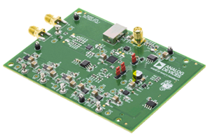
LTC1867CGN Demo Board | 16-Bit, 8-Channel 200ksps ADC (Requires DC2026)
Analog Devices Inc.Demonstration circuit 806A features the LTC1867 Octal 16-bit ADC. The LTC1867 can be software programmed for a unipolar 0V to 4.096V or bipolar ±2.048V input range. The 8 channel multiplexer can be programmed for 8 single-ended inputs with respect to ground, 7 single-ended inputs with respect to the COM/CH7 pin, 4 differential inputs, or any combination of these.
LTC2606 16-Bit, I2C VOUT DAC Demo Board (Requires DC590)
Analog Devices Inc.DC812A: Demo Board for the LTC2606 16-Bit Rail-to-Rail DACs with I2C Interface.
LTC2292IUP | MUX Dual ADC, VDD = +3.0V, 40Msps, 12Bit, 1MHz < AIN < 70MHz, (Requires DC718)
Analog Devices Inc.DC816A-J: Demo Board for the LTC2292 Dual 12-Bit, 40Msps Low Power 3V ADCs.
LTC2287IUP | MUX Dual ADC, VDD = +3.0V, 40Msps 10-Bit 1MHz < AIN < 70MHz, (Requires DC718)
Analog Devices Inc.DC816A-Q: Demo Board for the LTC2287 Dual 10-Bit, 40Msps Low Noise 3V ADCs.
ADP2165-EVALZ
Analog Devices Inc.The ADP2165/ADP2166 are high efficiency, current modecontrol, step-down dc-to-dc regulators with an integrated 19 m?high-side FET and a 15 m? synchronous rectified FET. TheADP2165/ADP2166 combine a small size, 4 mm ? 4 mm LFCSPpackage with an accurate current limit, resulting in a smallerinductor size and a high power density, point of load solution.Key features include precision enable, power-good monitor,and output voltage tracking to facilitate robust sequencing.The switching frequency can be programmed from 250 kHzto 1.4 MHz, or it can be fixed at 620 kHz or 1.2 MHz. Thesynchronization function allows the switching frequency tosynchronize to an external clock, minimizing theelectromagnetic interference (EMI) of the system.The ADP2165/ADP2166 are designed to be extremely flexiblewith the addition of a minimal amount of external componentsto program soft start and control loop compensation.he ADP2165/ADP2166 are supplied from an input voltage of2.7 V to 5.5 V. Output voltage options include 3.3 V, 2.5 V, 1.8 V,1.5 V, 1.2 V, or 1.0 V fixed outputs and adjustable options capableof supporting an output voltage range from 0.6 V to 90% of theinput voltage. Protection features include undervoltage lockout(UVLO), overvoltage protection (OVP), overcurrent protection(OCP), and thermal shutdown (TSD) for robust performance.The ADP2165/ADP2166 operate over the ?40?C to +125?Cjunction temperature range and are available in a 24-leadLFCSP package.Applications Point of load regulation Communications and networking High end consumer Industrial, instrumentation, and healthcare
ADP2386BB-EVALZ
Analog Devices Inc.The ADP2386 is a synchronous step-down, dc-to-dc regulator with an integrated 44 m?, high-side power MOSFET and an 11 m?, synchronous rectifier MOSFET to provide a high efficiency solution in a compact 4 mm ? 4 mm LFCSP package. This device uses a peak current mode, constant frequency pulse-width modulation (PWM) control scheme for excellent stability and transient response. The switching frequency of the ADP2386 can be programmed between 200 kHz to 1.4 MHz. To minimize system noise, the synchronization function allows the switching frequency to be synchronized to an external clock.The ADP2386 requires minimal external components and operates from an input voltage of 4.5 V to 20 V. The output voltage can be adjusted from 0.6 V to 90% of the input voltage and delivers up to 6 A of continuous current. Each IC draws less than 110 ?A current from the input source when it is disabled.This regulator targets high performance applications that require high efficiency and design flexibility. External compensation and an adjustable soft start function provide design flexibility. The power-good output and precision enable input provide simple and reliable power sequencing.Other key features include undervoltage lockout (UVLO), overvoltage protection (OVP), overcurrent protection (OCP), short-circuit protection (SCP) and thermal shutdown (TSD).The ADP2386 operates over the ?40?C to +125?C junction temperature range and is available in a 24-lead, 4 mm ? 4 mm LFCSP package.Applications Communications infrastructure Networking and servers Industrial and instrumentation Healthcare and medical Intermediate power rail conversion DC-to-dc point-of-load applications
ADP2443-EVALZ
Analog Devices Inc.The ADP2443 is synchronous step-down, dc-to-dc regulator with an integrated 98 m?, high-side power metal oxide semicon-ductor field effect transistor (MOSFET) and a 35 m?, synchronous rectifier MOSFET to provide a high efficiency solution in a compact 4 mm ? 4 mm LFCSP package. The regulators operate from an input voltage range of 4.5 V to 36 V. The output voltage can be adjusted down to 0.6 V and deliver up to 3 A of continuous current. The fast 50 ns minimum on time allows the regulators convert high input voltage to low output voltage at high frequency.The ADP2443 uses an emulated current mode, constant frequency pulse-width modulation (PWM) control scheme for excellent stability and transient response. The switching frequency of the ADP2443 can be programmed from 200 kHz to 1.8 MHz. The synchronization function allows the switching frequency be syn-chronized with an external clock to minimize the system noise.The ADP2443 targets high performance applications that require high efficiency and design flexibility. External compensation and an adjustable soft start function provide design flexibility. The power-good output and precision enable input provide simple and reliable power sequencing.Other key features include undervoltage lockout (UVLO), overvoltage protection (OVP), overcurrent protection (OCP), short-circuit protection (SCP), and thermal shutdown (TSD).The ADP2443 operates over the ?40?C to +125?C operating junction temperature range and is available in a 24-lead, 4 mm ? 4 mm LFCSP package.Applications Intermediate power rail conversion Multicell battery powered systems Process control and industrial automation Healthcare and medical Networking and servers
ADP322CPZ-REDYKIT
Analog Devices Inc.The ADP322/ADP323 200 mA triple output LDOs combine high PSRR, low noise, low quiescent current, and low dropout voltage to extend the battery life of portable devices and are ideally suited for wireless applications with demanding performance and board space requirements.The ADP322/ADP323 PSRR is greater than 60 dB for frequencies as high as 100 kHz while operating with a low headroom voltage. The ADP322/ADP323 offer much lower noise performance than competing LDOs without the need for a noise bypass capacitor.The ADP322/ADP323 are available in a miniature 16-lead, 3 mm ? 3 mm LFCSP package and are stable with tiny 1 ?F ?30% ceramic output capacitors providing the smallest possible board area for a wide variety of portable power needs.The ADP322 is available in output voltage combinations ranging from 0.8 V to 3.3 V and offers overcurrent and thermal protection to prevent damage in adverse conditions. The ADP323 adjustable triple LDO can be configured for any output voltage between 0.5 V and 5 V with two resistors for each output.Applications Mobile phones Digital cameras and audio devices Portable and battery-powered equipment Portable medical devices Post dc-to-dc regulation
ADP5034-1-EVALZ
Analog Devices Inc.The ADP5034 combines two high performance buck regulators and two low dropout (LDO) regulators in a small, 24-lead 4 mm ? 4 mm LFCSP (QFN) to meet demanding performance and board space requirements.The high switching frequency of the buck regulators enables tiny multilayer external components and minimizes the board space. When the MODE pin is set high, the buck regulators operate in forced PWM mode. When the MODE pin is set low, the buck regulators operate in PWM mode when the load is around the nominal value. When the load current falls below a predefined threshold, the regulator operates in power save mode (PSM), improving the light-load efficiency.The two bucks operate out of phase to reduce the input capaci-tor requirement. The low quiescent current, low dropout voltage, and wide input voltage range of the ADP5034 LDOs extend the battery life of portable devices. The ADP5034 LDOs maintain power supply rejection greater than 60 dB for frequencies as high as 10 kHz while operating with a low headroom voltage.Regulators in the ADP5034 are activated though dedicated enable pins. The default output voltages can be externally set in the adjustable version, or factory programmable in the fixed voltage version, and can be set to a wide range of preset valuesAPPLICATIONSPower for processors, ASICS, FPGAs, and RF chipsetsPortable instrumentation and medical devicesSpace constrained devices
ADP5053-EVALZ
Analog Devices Inc.The ADP5053 combines four high performance buck regulators, a supervisory circuit, a watchdog timer, and a manual reset in a 48-lead LFCSP package that meets demanding performance and board space requirements. The device enables direct connection to high input voltages up to 15.0 V with no preregulators.Channel 1 and Channel 2 integrate high-side power MOSFET and low-side MOSFET drivers. External NFETs can be used in low-side power devices to achieve an efficiency optimized solution and deliver a programmable output current of 1.2 A, 2.5 A, or 4 A. Combining Channel 1 and Channel 2 in a parallel configuration can provide a single output with up to 8 A of current.Channel 3 and Channel 4 integrate both high-side and low-side MOSFETs to deliver an output current of 1.2 A.The switching frequency of the ADP5053 can be programmed or synchronized to an external clock. The ADP5053 contains a precision enable pin on each channel for easy power-up sequencing or adjustable UVLO threshold.The ADP5053 contains supervisory circuits that monitor the voltage level. The watchdog timer can generate a reset if the WDI pin is not toggled within a preset timeout period. Processor reset mode or system power on/off switch mode can be selected for manual reset functionality.Applications Small cell base stations FPGA and processor applications Security and surveillance Medical applications
ADP5054-EVALZ
Analog Devices Inc.The ADP5054 combines four high performance buck regulators in a 48-lead LFCSP package that meets demanding performance and board space requirements. The device enables direct connection to high input voltages of up to 15.5 V with no preregulators.Channel 1 and Channel 2 integrate high-side power metal-oxide semiconductor field effect transistors (MOSFETs) and low-side MOSFET drivers. External NFETs can be used in low-side power devices to achieve an efficiency optimized solution and to deliver a programmable output current of 2 A, 4 A, or 6 A. Combining Channel 1 and Channel 2 in a parallel configuration provides a single output with up to 12 A of current.Channel 3 and Channel 4 integrate both high-side and low-side MOSFETs to deliver an output current of 2.5 A. Combining Channel 3 and Channel 4 in a parallel configuration can provide a single output with up to 5 A of current.The switching frequency of the ADP5054 can be programmed or synchronized to an external clock from 250 kHz to 2 MHz, and an individual ?? frequency configuration is available for each channel.The ADP5054 contains an individual precision enable pin on each channel for easy power-up sequencing. The internal low 1/f noise reference is implemented in the ADP5054 for noise sensitive applications.Applications FPGA and processor applications Small cell base stations Security and surveillance Medical applications
ADP5055-EVALZ
Analog Devices Inc.The ADP5055 combines three high performance buck regulators in a 43-terminal land grid array (LGA) package to meet demanding performance and board space requirements. The device enables direct connection to high input voltages up to 18 V with no preregulators. All channels integrate both high-side and low-side power metal-oxide semiconductor field effect transistors (MOSFETs) to achieve an efficiency optimized solution. Channel 1 and Channel 2 deliver a programmable output current of 3.5 A or 7 A or provide a single output with up to 14 A of current in parallel operation. Channel 3 delivers a programmable output current of 1.5 A or 3 A.The switching frequency of the ADP5055 can be programmed or synchronized to an external clock. The ADP5055 contains an enable pin (ENx) on each channel for simple power-up sequencing or adjustable undervoltage lockout (UVLO) threshold.The ADP5055 integrates a high precision 8-bit digital-to-analog converter (DAC) to enable the output voltage dynamic voltage scaling (DVS) via the PMBus?-compatible, 2-wire interface. The PMBus interface provides other flexible configurations, such as start-up and shutdown sequence control, individual forced pulse-width modulation or power saving mode (FPWM or PSM) selection, an output discharge switch, and a power-good signal.The ADP5055 is rated at ?40?C to +150?C junction temperature. APPLICATIONS Small cell base stations Field programmable gate array (FPGA) and processor applications Security and surveillance Medical applications
ADP5070RE-EVALZ
Analog Devices Inc.The ADP5070 is a dual high performance dc-to-dc regulator that generates independently regulated positive and negative rails.The input voltage range of 2.85 V to 15 V supports a wide variety of applications. The integrated main switch in both regulators enables generation of an adjustable positive output voltage up to +39 V and a negative output voltage down to ?39 V below input voltage.The ADP5070 operates at a pin selected 1.2 MHz/2.4 MHz switching frequency. The ADP5070 can synchronize with an external oscillator from 1.0 MHz to 2.6 MHz to ease noise filtering in sensitive applications. Both regulators implement programmable slew rate control circuitry for the MOSFET driver stage to reduce electromagnetic interference (EMI).Flexible start-up sequencing is provided with the options of manual enable, simultaneous mode, positive supply first, and negative supply first.The ADP5070 includes a fixed internal or resistor programmable soft start timer to prevent inrush current at power-up. During shutdown, both regulators completely disconnect the loads from the input supply to provide a true shutdown.Other key safety features in the ADP5070 include overcurrent protection (OCP), overvoltage protection (OVP), thermal shutdown (TSD), and input undervoltage lockout (UVLO).The ADP5070 is available in a 20-lead LFCSP or in a 20-lead TSSOP and is rated for a ?40?C to +125?C junction temperature range.Applications Bipolar amplifiers, ADCs, DACs and multiplexers Charge-coupled device (CCD) bias supply Optical module supply RF power amplifier (PA) bias
ADP5071RE-EVALZ
Analog Devices Inc.The ADP5071 is a dual high performance dc-to-dc regulator that generates independently regulated positive and negative rails.The input voltage range of 2.85 V to 15 V supports a wide variety of applications. The integrated main switch in both regulators enables generation of an adjustable positive output voltage up to +39 V and a negative output voltage down to ?39 V below input voltage.The ADP5071 operates at a pin selected 1.2 MHz/2.4 MHz switching frequency. The ADP5071 can synchronize with an external oscillator from 1.0 MHz to 2.6 MHz to ease noise filtering in sensitive applications. Both regulators implement programmable slew rate control circuitry for the MOSFET driver stage to reduce electromagnetic interference (EMI).Flexible start-up sequencing is provided with the options of manual enable, simultaneous mode, positive supply first, and negative supply first.The ADP5071 includes a fixed internal or resistor programmable soft start timer to prevent inrush current at power-up. During shutdown, both regulators completely disconnect the loads from the input supply to provide a true shutdown.Other key safety features in the ADP5071 include overcurrent protection (OCP), overvoltage protection (OVP), thermal shutdown (TSD), and input undervoltage lockout (UVLO).The ADP5071 is available in a 20-lead LFCSP or in a 20-lead TSSOP and is rated for a ?40?C to +125?C junction temperature range.Applications Bipolar amplifiers, ADCs, DACs, and multiplexers Charge-coupled device (CCD) bias supply Optical module supply RF power amplifier (PA) bias
ADP5072CB-EVALZ
Analog Devices Inc.The ADP5072 is a dual, high performance dc-to-dc regulator that generates independently regulated positive and negative rails.The input voltage range of 2.85 V to 5.5 V supports a wide variety of applications. The integrated main switch in both regulators enables generation of an adjustable positive output voltage up to 35 V and a negative output voltage down to ?30 V.The ADP5072 operates at a pin selected 1.2 MHz or 2.4 MHz switching frequency. The ADP5072 can synchronize with an external oscillator from 1.0 MHz to 2.6 MHz to ease noise filtering in sensitive applications. Both regulators implement programmable slew rate control circuitry for the MOSFET driver stage to reduce electromagnetic interference (EMI). Flexible start-up sequencing is provided with the options of manual enable, simultaneous mode, positive supply first, and negative supply first.The ADP5072 includes a fixed internal or resistor programmable soft start timer to prevent inrush current at power-up.Other key safety features in the ADP5072 include overcurrent protection (OCP), overvoltage protection (OVP), thermal shutdown (TSD), and input undervoltage lockout (UVLO).The ADP5072 is available in a 20-ball WLCSP and is rated for a ?40?C to +125?C junction temperature range.Bipolar amplifiers, analog-to-digital converters (ADCs), digital-to-analog converters (DACs), and multiplexersCharge coupled device (CCD) bias suppliesOptical module suppliesRF power amplifier biasTime of flight module supplies
ADP5080CB-1-EVALZ
Analog Devices Inc.The ADP5080 is a fully integrated, high efficiency power solution for multicell lithium ion battery applications. The device can connect directly to the battery, which eliminates the need for preregulators and, therefore, increases the battery life of the system.The ADP5080 integrates two keep-alive LDO regulators, five synchronous buck regulators, a configurable four-switch buck boost regulator, and a high voltage LDO regulator. The ADP5080 is a highly integrated power solution that incorporates all power MOSFETs, feedback loop compensation, voltage setting resistor dividers, and discharge switches, as well as a charge pump to generate a global bootstrap voltage.All these features help to minimize the number of external components and PCB space required, providing significant advantages for portable applications. The switching frequency is selectable on each channel from 750 kHz to 2 MHz.Key functions for power applications, such as soft start, selectable preset output voltage, and flexible power-up and power-down sequences, are provided on chip and are programmable via the I2C interface with fused factory defaults. The ADP5080 is available in a 72-ball WLCSP 0.5 mm pitch package.APPLICATIONS DSLR cameras Non-reflex (mirrorless) cameras Portable instrumentation
ADP5091-1-EVALZ
Analog Devices Inc.The ADP5091/ADP5092 are intelligent, integrated energy harvesting, ultralow power management unit (PMU) solutions that convert dc power from PV cells or TEGs. These devices charge storage elements such as rechargeable Li-Ion batteries, thin film batteries, super capacitors, or conventional capacitors, and power up small electronic devices and battery free systems.The ADP5091/ADP5092 provide efficient conversion of the harvested limited power from a 6 ?W to 600 mW range with submicrowatt operation losses. With the internal cold start circuit, the regulator can start operating at an input voltage as low as 380 mV. After cold startup, the regulator is functional at an input voltage range of 0.08 V to 3.3 V. An additional 150 mA regulated output can be programmed by an external resistor divider or the VID pin.The MPPT control keeps the input voltage ripple in a fixed range to maintain stable dc-to-dc boost conversion. The dynamic sensing mode and no sensing mode, both programming regulation points of the input voltage, allow extraction of the highest possible energy from the harvester. A programmable minimum operation threshold enables boost shutdown during a low input condition.As a low light indicator for a microprocessor, the LLD pin of the ADP5091 is the MINOP comparator output. However, the REG_GOOD flag of the ADP5092 monitors the REG_OUT voltage. In addition, the DIS_SW pin can temporarily shut down the boost regulator and is RF transmission friendly.The charging control function of the ADP5091/ADP5092 protects the rechargeable energy storage, which is achieved by monitoring the battery voltage with the programmable charging termination voltage and the shutdown discharging voltage. In addition, a programmable PGOOD flag monitors the SYS voltage.An optional primary cell battery can be connected and managed by an integrated power path management control block that is programmable to switch the power source from the energy harvester, rechargeable battery, and primary cell battery.The ADP5091/ADP5092 are available in a 24-lead LFCSP and are rated for a ?40?C to +125?C temperature range.Applications Photovoltaic (PV) cell energy harvesting Thermoelectric generators (TEGs) energy harvesting Industrial monitoring Self powered wireless sensor devices Portable and wearable devices with energy harvesting
ADP5585CP-EVALZ
Analog Devices Inc.The ADP5585 is a 10I/O port expander with built-in keypad matrix decoder, programmable logic, reset generator, and PWM generator. I/O expander ICs are used in portable devices (phones, remote controls, & cameras) and non-portable applications (healthcare, industrial & instrumentation). I/O expanders can be used to increase the number of I/Os available to a processor or to reduce the number of I/Os required through interface connectors for front panel designs.The ADP5585 handles all key scanning and decoding and can flag the main processor via an interrupt line that new key events have occurred. GPI changes and logic changes can also be tracked as events via the FIFO, eliminating the need to monitor different registers for event changes. The ADP5585 is equipped with a FIFO to store up to 16 events. Events can be read back by the processor via an I2C compatible interface.The ADP5585 frees up the main processor from having to monitor the keypad, thereby reducing power consumption and/or increasing processor bandwidth for performing other functions.The programmable logic functions allow common logic requirements to be integrated as part of the GPIO expander, saving board area and cost.APPLICATIONS Keypad entries and input/output expansion capabilities Smart phones, remote controls, and cameras Healthcare, industrial, and instrumentation
ADP5600CP-EVALZ
Analog Devices Inc.The ADP5600 is an interleaved charge pump inverter with an integrated, negative, low dropout (LDO) linear regulator. The interleaved charge pump inverter exhibits reduced output voltage ripple and reflected input current noise over conventional inductive or conventional capacitive based solutions. The integrated LDO provides a rail with good regulation at sufficient power supply rejection ratio (PSRR).The ADP5600 charge pump operates via resistor programming or external clock synchronization at switching frequency range of 100 kHz to 1 MHz. Operating at a higher switching frequency allows the use of small input, output, and fly capacitors. To combine the high switching frequency with internal field effect transistors (FETs), compensation, and soft start gives a best-in-class total solution size for negative rail generation.The ADP5600 also features comprehensive fault protection for robust applications. These protections include overload protection, shorted fly capacitor protection, undervoltage lockout (UVLO), and thermal shutdown. For easy sequencing, the ADP5600 has a power-good pin.The integrated LDO of the ADP5600 uses an advanced proprie-tary architecture to provide high power supply rejection. It also achieves decent line and load transient response with only a small 2.2 ?F ceramic output capacitor. The output can be configured via the SEL1 and SEL2 pins to one of four fixed output voltages and is adjustable from ?0.505 V to ?VIN + 0.5 V via an external feedback divider.APPLICATIONSPowering the negative rail on bipolar/split supply ADC/DAC/AMP/mux applications
ADP7102CP-EVALZ
Analog Devices Inc.The ADP7102 is a CMOS, low dropout linear regulator that operates from 3.3 V to 20 V and provides up to 300 mA of output current. This high input voltage LDO is ideal for regulation of high performance analog and mixed signal circuits operating from 19 V to 1.22 V rails. Using an advanced proprietary architecture, it provides high power supply rejection, low noise, and achieves excellent line and load transient response with just a small 1 ?F ceramic output capacitor. The ADP7102 is available in seven fixed output voltage options and an adjustable version, which allows output voltages that range from 1.22 V to VIN ? VDO via an external feedback divider. The ADP7102 output noise voltage is 15 ?V rms and is independent of the output voltage. A digital power good output allows power system monitors to check the health of the output voltage. A user programmable precision undervoltage lockout function facilitates sequencing of multiple power supplies. The ADP7102 is available in 8-lead, 3 mm ? 3 mm LFCSP and 8-lead SOIC packages. The LFCSP offers a very compact solution and also provides excellent thermal performance for applications requiring up to 300 mA of output current in a small, low-profile footprint. APPLICATIONS Regulation to noise sensitive applications: ADC, DAC circuits, precision amplifiers, high frequency oscillators, clocks, and phase-locked loops Communications and infrastructure Medical and healthcare Industrial and instrumentation


