
DC2002A
Analog Devices Inc.The LTC3774 is a dual PolyPhase? current mode synchronous step-down switching regulator controller that drives power blocks, DRMOS or external gate drivers and power MOSFETs. It offers an LTC-proprietary technique that enhances the signal-to-noise ratio of the current sense signal, allowing the use of inductors with very low DC winding resistances as the current sense element for maximum efficiency and reduced jitter.The maximum current sense voltage is programmable from 10mV to 30mV. High speed, low offset remote sense differential amplifiers and a precise 0.6V reference provide accurate output voltages between 0.6V and 3.5V from a wide 4.5V to 38V input supply range. Soft recovery from output shorts or overcurrent minimizes output overshoot. Burst Mode? operation, continuous and pulse-skipping modes are supported. The constant operating frequency can be synchronized to an external clock or linearly programmed from 200kHz to 1.2MHz. Up to six LTC3774 controllers can be paralleled for 1-, 2-, 3-, 4-, 6-, 8- or 12-phase operation.The LTC3774 is available in a 36-lead (5mm ? 6mm) QFN package.Applications Computer Systems Telecom and Datacom Systems Industrial Equipment DC Power Distribution Systems

DC2003A
Analog Devices Inc.The LTC3622 is a dual 1A output, high efficiency synchronous monolithic step-down regulator capable of operating from input supplies up to 17V. The switching frequency is fixed to 1MHz or 2.25MHz with a ?50% synchronization range to an external clock. The regulator features ultralow quiescent current and high efficiency over a wide output voltage range.The step-down regulators operate from an input voltage range of 2.7V to 17V and provide an adjustable output from 0.6V to VIN while delivering up to 1A of output current. A user-selectable mode input is provided to allow the user to trade off ripple noise for light load efficiency. Burst Mode? operation provides the highest efficiency at light loads, while pulse-skipping mode provides the lowest ripple noise. The switching regulators can be synchronized to an external clock. Furthermore, fixed VOUT options are available to eliminate the external feedback resistors.? LTC3622 Options Part Name Frequency VOUT LTC3622 1.00MHz Adjustable LTC3622-2 2.25MHz Adjustable LTC3622-23/5 2.25MHZ 5V/3.3V ?Applications Battery Powered Systems Point-of-Load Supplies Portable ? Handheld Scanners

DC2007A-A
Analog Devices Inc.The LTM4630 is a dual 18A or single 36A output switching mode step-down DC/DC ?Module? (power module) regulator. Included in the package are the switching controllers, power FETs, inductors, and all supporting components. Operating from an input voltage range of 4.5V to 15V, the LTM4630 supports two outputs each with an output voltage range of 0.6V to 1.8V, each set by a single external resistor. Its high efficiency design delivers up to 18A continuous current for each output. Only a few input and output capacitors are needed. The LTM4630 is pin compatible with the LTM4620 and LTM4620A (dual 13A, single 26A) and the LTM4628 (dual 8A, single 16A).The device supports frequency synchronization, multiphase operation, Burst Mode operation and output voltage tracking for supply rail sequencing and has an onboard temperature diode for device temperature monitoring. High switching frequency and a current mode architecture enable a very fast transient response to line and load changes without sacrificing stability.Fault protection features include overvoltage and overcurrent protection. The LTM4630 is offered in 16mm ? 16mm ? 4.41mm LGA and 16mm ? 16mm ? 5.01mm BGA packages. The LTM4630 is ROHS compliant.? Features Vout LTM4630 0.6V to 1.8V LTM4630-1 0.8% DC and 3% Transient Accuracy 0.6V to 1.8V LTM4630A Higher Light Load Efficiency 0.6V to 5.3V Applications Telecom and Networking Equipment Storage and ATCA Cards Industrial Equipment
LTM4630 Demo Board | 140A Polyphase Step-Down (4x LTM4630), 4.5V ≤ VIN ≤ 15V, VOUT = 0.9V to 1.8V @ 140A
Analog Devices Inc.Demonstration circuit 2007A-C features a PolyPhase® design using the LTM4630EV, the high efficiency, high density, dual 18A, switch mode step-down power μModule® regulator. The input voltage is from 4.5V to 15V. The output voltage is jumper selectable from 0.9V to 1.8V. The DC2007A-C can deliver a nominal 140A output current. As explained in the data sheet, output current derating is necessary for certain VIN, VOUT, and thermal conditions. The LTM4630 on the DC2007A-C always operates in continuous conduction mode. The switching frequency can be programmed through a resistor or can be synchronized to an external clock signal. The board allows the user to program how its output voltage ramps up and down through the TRACK pin.

DC2026C-KIT
Analog Devices Inc.The LTC2607/LTC2617/LTC2627 are dual 16-, 14- and 12-bit, 2.7V to 5.5V rail-to-rail voltage output DACs in a 12-lead DFN package. They have built-in high performance output buffers and are guaranteed monotonic.These parts establish new board-density benchmarks for 16- and 14-bit DACs and advance performance standards for output drive and load regulation in single-supply, voltage-output DACs.The parts use a 2-wire, I2C compatible serial interface. The LTC2607/LTC2617/LTC2627 operate in both the standard mode (clock rate of 100kHz) and the fast mode (clock rate of 400kHz). An asynchronous DAC update pin (LDAC) is also included.The LTC2607/LTC2617/LTC2627 incorporate a power-on reset circuit. During power-up, the voltage outputs rise less than 10mV above zero scale; and after power-up, they stay at zero scale until a valid write and update take place. The power-on reset circuit resets the LTC2607-1/LTC2617-1/ LTC2627-1 to mid-scale. The voltage outputs stay at midscale until a valid write and update takes place.Applications Mobile Communications Process Control and Industrial Automation Instrumentation Automatic Test Equipment

LTC4364DE-1 Demoboard: 12V Surge Stopper with Ideal Diode, Latch Off
Analog Devices Inc.DC2027A-A: Demo Board for the LTC4364 Surge Stopper with Ideal Diode.

DC2028A
Analog Devices Inc.The LTC2977 is an 8-channel Power System Manager used to sequence, trim (servo), margin, supervise, manage faults, provide telemetry and create fault logs. PMBus commands support power supply sequencing, precision point-of-load voltage adjustment and margining. DACs use a proprietary soft-connect algorithm to minimize supply disturbances. Supervisory functions include overvoltage and undervoltage threshold limits for eight power supply output channels and one power supply input channel, as well as over and under temperature limits. Programmable fault responses can disable the power supplies with optional retry after a fault is detected. Faults that disable a power supply can automatically trigger black box EEPROM storage of fault status and associated telemetry. An internal 16-bit ADC monitors eight output voltages, one input voltage, and die temperature. In addition, odd numbered channels can be configured to measure the voltage across a current sense resistor. A programmable watchdog timer monitors microprocessor activity for a stalled condition and resets the microprocessor if necessary. A single wire bus synchronizes power supplies across multiple LTC Power System Management (PSM) devices. Configuration EEPROM with ECC supports autonomous operation without additional software.APPLICATIONS Computers and Network Servers Industrial Test and Measurement High Reliability Systems Medical Imaging Video

DC2038A-H
Analog Devices Inc.The LTC4162-S is an advanced monolithic synchronous step-down switching battery charger and PowerPath? manager that seamlessly manages power distribution between input sources such as wall adapters, backplanes, solar panels, etc., and a lead-acid battery.A high resolution measurement system provides extensive telemetry information for circuit voltages, currents, battery resistance and temperature which can all be read back over the I2C port. The I2C port can also be used to configure many charging parameters including charging voltages and currents, termination algorithms and numerous system status alerts.The LTC4162-S can charge 6V, 12V, 18V and 24V lead-acid batteries with as much as 3.2A of charge current.The power path topology decouples the output voltage from the battery allowing a portable product to start up instantly under very low battery voltage conditions.The LTC4162-S is available in a thermally enhanced 28-pin 4mm ? 5mm ? 0.75mm QFN surface mount package.Applications Medical Instruments USB-C Power Delivery Industrial Handhelds Ruggedized Notebook Tablet Computers

LT4276B/LT4321 Demo Board | PoE+(25W, 24V/1A) PD with DC/DC and Ideal Diode Bridge
Analog Devices Inc.Demonstration circuit 2046A-D is a PoE powered device (PD) with an isolated power supply using synchronous flyback topology, featuring the LT4276 and ideal diode bridge controller (LT4321).
LT4276B/LT4321 Demo Board | PoE+ (25W, 12V/1.9A) PD with DC/DC, Ideal Diode Bridge and 9V-57V AUX
Analog Devices Inc.Demonstration circuit 2047A-A is an IEEE802.3at compliant Power over Ethernet (PoE) Powered Device (PD) with support for 9-57VDC and 24VAC auxiliary supply input. It features the LT4276 PD interface and switching regulator controller, the LT4321 PoE ideal diode bridge controller, and the LT4320 ideal diode bridge controller.

LT1776CS8 | High Voltage, High Efficiency, Step-Down Switching Regulator, 7V to 60VIN, 3.3V and 5V @ 0.5A Out (Thru-hole Input Cap)
Analog Devices Inc.DC204A-B: Demo Board for the LT1776 Wide Input Range, High Efficiency, Step-Down Switching Regulator.

DC2050A
Analog Devices Inc.The LT3753 is a current mode PWM controller optimized for an active clamp forward converter topology, allowing up to 100V input operation.A programmable volt-second clamp allows primary switch duty cycles above 50% for high switch, transformer and rectifier utilization. Active clamp control reduces switch voltage stress and increases efficiency. A synchronous output is available for controlling secondary side synchronous rectification.The LT3753 is available in a 38-lead plastic TSSOP package with missing pins for high voltage spacings.Applications Industrial, Automotive and Military Systems 48V Telecommunication Isolated Power Supplies

LT4363IDE-1 Demo Board: 12V System ISO-7637-2 Surge Stopper, Latch-Off Version
Analog Devices Inc.DC2062A-A: Demo Board for LT4363 High Voltage Surge Stopper with Current Limit.

DC2066A
Analog Devices Inc.The LTM4677 is a dual 18A or single 36A step-down ?Module? (power module) DC/DC regulator with 40ms turn0on time. It features remote configurability and telemetry-monitoring of power management parameters over PMBus?an open standard I2C-based digital interface protocol. The LTM4677 is comprised of fast analog control loops, precision mixedsignal circuitry, EEPROM, power MOSFETs, inductors and supporting components.The LTM4677?s 2-wire serial interface allows outputs to be margined, tuned and ramped up and down at programmable slew rates with sequencing delay times. Input and output currents and voltages, output power, temperatures, uptime and peak values are readable. Custom configuration of the EEPROM contents is not required. At start-up, output voltages, switching frequency, and channel phase angle assignments can be set by pin-strapping resistors. The LTpowerPlay? GUI and DC1613 USB-to-PMBus converter and demo kits are available.The LTM4677 is pin compatible with the LTM4676A (dual 13A) and is offered in a 16mm ? 16mm ? 5.01mm BGA package available with SnPb or RoHS compliant terminal finish.APPLICATIONS System Optimization, Characterization and Data Mining?in Prototype, Production and Field Environments Telecom, Datacom, and Storage Systems

DC2071A-B
Analog Devices Inc.The LTC2372-18 is a low noise, high speed, 8-channel 18-bit successive approximation register (SAR) ADC. Operating from a single 5V supply, the LTC2372-18 has a highly configurable, low crosstalk 8-channel input multiplexer, supporting fully differential, pseudo-differential unipolar and pseudo-differential bipolar analog input ranges. The LTC2372-18 achieves ?2.75LSB INL (maximum) in all input ranges, no missing codes at 18-bits and 100dB (fully differential)/ 95dB (pseudo-differential) SNR (typical).The LTC2372-18 has an onboard low drift (20ppm/?C max) 2.048V temperature-compensated reference and a single-shot capable reference buffer. The LTC2372-18 also has a high speed SPI-compatible serial interface that supports 1.8V, 2.5V, 3.3V and 5V logic through which a sequencer with a depth of 16 may be programmed. An internal oscillator sets the conversion time, easing external timing considerations. The LTC2372-18 dissipates only 27mW and automatically naps between conversions, leading to reduced power dissipation that scales with the sampling rate. A sleep mode is also provided to reduce the power consumption of the LTC2372-18 to 300?W for further power savings during inactive periods.Applications Programmable Logic Controllers Industrial Process Control High Speed Data Acquisition Portable or Compact Instrumentation ATE

AD9162-FMC-EBZ
Analog Devices Inc.The AD9162 is a high performance, 16-bit digital-to-analog converter (DAC) that supports data rates to 6 GSPS. The DAC core is based on a quad-switch architecture coupled with a 2? interpolator filter that enables an effective DAC update rate of up to 12 GSPS in some modes. The high dynamic range and bandwidth makes these DACs ideally suited for the most demanding high speed radio frequency (RF) DAC applications.In baseband mode, wide bandwidth capability combines with high dynamic range to support DOCSIS 3.1 cable infrastructure compliance from the minimum of two carriers to full maximum spectrum of 1.794 GHz. A 2? interpolator filter (FIR85) enables the AD9161/AD9162 to be configured for lower data rates and converter clocking to reduce the overall system power and ease the filtering requirements. In Mix-Mode? operation, the AD9161/AD9162 can reconstruct RF carriers in the second and third Nyquist zones up to 7.5 GHz while still maintaining exceptional dynamic range. The output current can be programmed from 8 mA to 38.76 mA. The AD9161/AD9162 data interface consists of up to eight JESD204B serializer/deserializer (SERDES) lanes that are programmable in terms of lane speed and number of lanes to enable application flexibility.A serial peripheral interface (SPI) can configure the AD9161/AD9162 and monitor the status of all registers. The AD9161/AD9162 are offered in an 165-ball, 8.0 mm ? 8.0 mm, 0.5 mm pitch, CSP_BGA package and in an 169-ball, 11 mm ? 11 mm, 0.8 mm pitch, CSP_BGA package, including a leaded ball option for the AD9162.Product Highlights High dynamic range and signal reconstruction bandwidth supports RF signal synthesis of up to 7.5 GHz. Up to eight lanes JESD204B SERDES interface flexible in terms of number of lanes and lane speed. Bandwidth and dynamic range to meet DOCSIS 3.1 compliance with margin.Applications Broadband communications systems DOCSIS 3.1 cable modem termination system (CMTS)/video on demand (VOD)/edge quadrature amplitude modulation (EQAM) Wireless communications infrastructure W-CDMA, LTE, LTE-A, point to point Instrumentation, automatic test equipment (ATE) Radars and jammers

AD9171-FMC-EBZ
Analog Devices Inc.The AD9171 is a high performance, dual, 16-bit digital-to-analog converter (DAC) that supports DAC sample rates to 6.2 GSPS. The device features an 8-lane, 15.4 Gbps JESD204B data input port, a high performance, on-chip DAC clock multiplier, and digital signal processing capabilities targeted at single-band direct to radio frequency (RF) wireless applications.The AD9171 features one complex data input channels per RF DAC. Each data input channel includes a configurable gain stage, an interpolation filter, and a channel numerically controlled oscillator (NCO) for flexible, frequency planning. The device supports up to a 516 MSPS complex data rate per input channel.The AD9171 is available in a 144-ball BGA_ED package.PRODUCT HIGHLIGHTS Supports one complex data input channel per RF DAC at a maximum complex input data rate of 513 MSPS with 12-bitresolution and 516 MSPS with 16-bit resolution options. There is one independent NCO per input channel. Low power dual converter decreases the amount of power consumption needed in high bandwidth and multichannel applications.?APPLICATIONS Wireless communications infrastructure Single-band base station radios Instrumentation, automatic test equipment (ATE)

AD9208-DUAL-EBZ
Analog Devices Inc.The AD9208 is a dual, 14-bit, 3 GSPS analog-to-digital converter (ADC). The device has an on-chip buffer and a sample-and-hold circuit designed for low power, small size, and ease of use. This product is designed to support communications applications capable of direct sampling wide bandwidth analog signals of up to 5 GHz. The ?3 dB bandwidth of the ADC input is 9 GHz. The AD9208 is optimized for wide input bandwidth, high sampling rate, excellent linearity, and low power in a small package.The dual ADC cores feature a multistage, differential pipelined architecture with integrated output error correction logic. Each ADC features wide bandwidth inputs supporting a variety of user-selectable input ranges. An integrated voltage referenceeases design considerations. The analog input and clock signals are differential inputs. The ADC data outputs are internally connected to four digital downconverters (DDCs) through a crossbar mux. Each DDC consists of up to five cascaded signalprocessing stages: a 48-bit frequency translator (numerically controlled oscillator (NCO)), and up to four half-band decimationfilters. The NCO has the option to select preset bands over the general-purpose input/output (GPIO) pins, which enables the selection of up to three bands. Operation of the AD9208 between the DDC modes is selectable via SPI-programmable profiles.In addition to the DDC blocks, the AD9208 has several functions that simplify the automatic gain control (AGC) function in acommunications receiver. The programmable threshold detector allows monitoring of the incoming signal power using the fast detect control bits in Register 0x0245 of the ADC. If the input signal level exceeds the programmable threshold, the fast detect indicator goes high. Because this threshold indicator has low latency, the user can quickly turn down the system gain to avoidan overrange condition at the ADC input. In addition to the fast detect outputs, the AD9208 also offers signal monitoring capability. The signal monitoring block provides additional information about the signal being digitized by the ADC.The user can configure the Subclasss 1 JESD204B-based high speed serialized output in a variety of one-lane, two-lane, four-lane, and eight-lane configurations, depending on the DDC configuration and the acceptable lane rate of the receiving logic device. Multidevice synchronization is supported through the SYSREF? and SYNCINB? input pins.The AD9208 has flexible power-down options that allow significant power savings when desired. All of these features canbe programmed using a 3-wire serial port interface (SPI).The AD9208 is available in a Pb-free, 196-ball BGA, specified over the ?40?C to +85?C ambient temperature range. Thisproduct is protected by a U.S. patent.Note that throughout this data sheet, multifunction pins, such as FD_A/GPIO_A0, are referred to either by the entire pin name or by a single function of the pin, for example, FD_A, when only that function is relevant.Product Highlights Wide, input ?3 dB bandwidth of 9 GHz supports direct radio frequency (RF) sampling of signals up to about 5 GHz. Four integrated, wideband decimation filter and NCO blocks supporting multiband receivers. Fast NCO switching enabled through GPIO pins. A SPI controls various product features and functions to meet specific system requirements. Programmable fast overrange detection and signal monitoring. On-chip temperature dioide for system thermal management. 12mm ? 12mm 196-Lead BGAApplications Diversity multiband, multimode digital receivers 3G/4G, TD-SCDMA, W-CDMA, GSM, LTE, LTE-A Electronic test and measurement systems Phased array radar and electronic warfare DOCSIS 3.0 CMTS upstream receive paths HFC digital reverse path receivers

AD9212-65EBZ
Analog Devices Inc.The AD9212 is an octal, 10-bit, 40 MSPS/65 MSPS ADC with an on-chip sample-and-hold circuit designed for low cost, low power,small size, and ease of use. Operating at a conversion rate of up to 65 MSPS, it is optimized for outstanding dynamic performance and low power in applications where a small package size is critical.The ADC requires a single 1.8 V power supply and LVPECL-/ CMOS-/LVDS-compatible sample rate clock for full performanceoperation. No external reference or driver components arerequired for many applications.The ADC automatically multiplies the sample rate clock forthe appropriate LVDS serial data rate. A data clock (DCO)for capturing data on the output and a frame clock (FCO) for signaling a new output byte are provided. Individual channelpower-down is supported and typically consumes less than 2 mW when all channels are disabled.The ADC contains several features designed to maximizeflexibility and minimize system cost, such as programmableclock and data alignment and programmable digital test patterngeneration. The available digital test patterns include built-in deterministic and pseudorandom patterns, along with custom user-defined test patterns entered via the serial port interface (SPI).The AD9212 is available in a RoHS-compliant, 64-lead LFCSP. It isspecified over the industrial temperature range of ?40?C to +85?C.PRODUCT HIGHLIGHTS Small Footprint. Eight ADCs are contained in a small package. Low Power of 100 mW per Channel at 65 MSPS. Ease of Use. A data clock output (DCO) operates up to 300 MHz and supports double data rate (DDR) operation. User Flexibility. SPI control offers a wide range of flexible features to meet specific system requirements. Pin-Compatible Family. This includes the AD9222 (12-bit) and AD9252 (14-bit).APPLICATIONS Medical imaging and nondestructive ultrasound Portable ultrasound and digital beam-forming systems Quadrature radio receivers Diversity radio receivers Tape drives Optical networking Test equipment
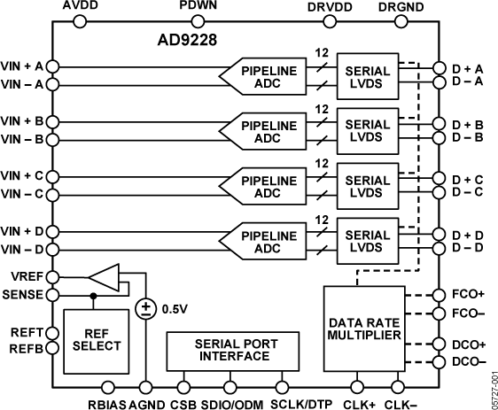
AD9228-65EBZ
Analog Devices Inc.The AD9228 is a quad, 12-bit, 40/65 MSPS analog-to-digital converter (ADC) with an on-chip sample-and-hold circuit designed for low cost, low power, small size, and ease of use. The product operates at a conversion rate of up to 65 MSPS and is optimized for outstanding dynamic performance and low power in applications where a small package size is critical. The ADC requires a single 1.8 V power supply and LVPECL-/ CMOS-/LVDS-compatible sample rate clock for full performance operation. No external reference or driver components are required for many applications. The ADC automatically multiplies the sample rate clock for the appropriate LVDS serial data rate. A data clock output (DCO) for capturing data on the output and a frame clock output (FCO) for signaling a new output byte are provided. Individual channel power-down is supported and typically consumes The ADC contains several features designed to maximize flexibility and minimize system cost, such as programmable clock and data alignment and programmable digital test pattern generation. The available digital test patterns include built-in deterministic and pseudorandom patterns, along with custom user-defined test patterns entered via the serial port interface (SPI). The AD9228 is available in an RoHS compliant, 48-lead LFCSP. It is specified over the industrial temperature range of ?40?C to +85?C.PRODUCT HIGHLIGHTSSmall Footprint. Four ADCs are contained in a small, space-saving package. Low power of 119 mW/channel at 65 MSPS. Ease of Use. A data clock output (DCO) is provided that operates at frequencies of up to 390 MHz and supports double data rate (DDR) operation.User Flexibility. The SPI control offers a wide range of flexible features to meet specific system requirements. Pin-Compatible Family. This includes the AD9287 (8-bit), AD9219 (10-bit), and AD9259 (14-bit).?APPLICATIONSMedical imaging and nondestructive ultrasound Portable ultrasound and digital beam-forming systemsQuadrature radio receivers Diversity radio receivers Tape drives Optical networking Test equipment


