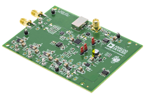
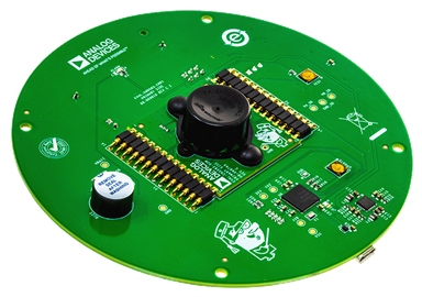
AD9655-125EBZ
Analog Devices Inc.The AD9655 is a dual, 16-bit, 125 MSPS analog-to-digital converter (ADC) with an on-chip sample-and-hold circuit designed for low cost, low power, small size, and ease of use. The product operates at a conversion rate of up to 125 MSPS and is optimized for outstanding dynamic performance and low power in applications where a small package size is critical.The ADC requires a single 1.8 V power supply and an LVPECL-/CMOS-/LVDS-compatible sample rate clock for full performance operation. External reference or driver components are not required for many applications.The ADC automatically multiplies the sample rate clock for the appropriate LVDS serial data rate. A data clock output (DCO) for capturing data on the output and a frame clock output (FCO) for signaling a new output byte are provided. Individual channel power-down is supported.The AD9655 typically consumes less than 2 mW in SPI powerdown mode. The available digital test patterns include built-in deterministic and pseudorandom patterns, along with custom user-defined test patterns entered via the serial port interface (SPI).The AD9655 is available in a RoHS-compliant, 32-lead LFCSP. It is specified over the industrial temperature range of ?40?C to +85?C. This device is protected by a U.S. patent.PRODUCT HIGHLIGHTS Small Footprint. Two ADCs are contained in a small, spacesaving package. Pin compatible to the AD9645 14-bit and AD9635 12-bit dual ADCs. Ease of use. A DCO operates at frequencies of up to 500 MHz and supports double data rate (DDR) operation. User Flexibility. The SPI control offers a wide range of flexible features to meet specific system requirements.APPLICATIONS Communications Diversity radio systems Multimode digital receivers GSM, EDGE, W-CDMA, LTE, CDMA2000, WiMAX, TD-SCDMA I/Q demodulation systems Smart antenna systems Broadband data applications Battery-powered instruments Hand held scope meters Portable medical imaging Radar/LIDAR
AD9680-500EBZ
Analog Devices Inc.The AD9680 is a dual, 14-bit, 1.25 GSPS/1 GSPS/820 MSPS/500 MSPS analog-to-digital converter (ADC). The device has an on-chip buffer and sample-and-hold circuit designed for low power, small size, and ease of use. This device is designed for sampling wide bandwidth analog signals of up to 2 GHz. The AD9680 is optimized for wide input bandwidth, high sampling rate, excellent linearity, and low power in a small package.The dual ADC cores feature a multistage, differential pipelined architecture with integrated output error correction logic. Each ADC features wide bandwidth inputs supporting a variety of user-selectable input ranges. An integrated voltage reference eases design considerations.The analog input and clock signals are differential inputs. Each ADC data output is internally connected to two digital down-converters (DDCs). Each DDC consists of up to five cascaded signal processing stages: a 12-bit frequency translator (NCO), and four half-band decimation filters. The DDCs are bypassed by default.In addition to the DDC blocks, the AD9680 has several functions that simplify the automatic gain control (AGC) function in the communications receiver. The programmable threshold detector allows monitoring of the incoming signal power using the fast detect output bits of the ADC. If the input signal level exceeds the programmable threshold, the fast detect indicator goes high. Because this threshold indicator has low latency, the user can quickly turn down the system gain to avoid an overrange condition at the ADC input.Users can configure the Subclass 1 JESD204B-based high speed serialized output in a variety of one-, two-, or four-lane configurations, depending on the DDC configuration and the acceptable lane rate of the receiving logic device. Multiple device synchronization is supported through the SYSREF? and SYNCINB? input pins.The AD9680 has flexible power-down options that allow significant power savings when desired. All of these features can be programmed using a 1.8 V to 3.3 V capable, 3-wire SPI.The AD9680 is available in a Pb-free, 64-lead LFCSP and is specified over the ?40?C to +85?C industrial temperature range. This product is protected by a U.S. patent.PRODUCT HIGHLIGHTS Wide full power bandwidth supports IF sampling of signals up to 2 GHz. Buffered inputs with programmable input termination eases filter design and implementation. Four integrated wideband decimation filters and numerically controlled oscillator (NCO) blocks supporting multiband receivers. Flexible serial port interface (SPI) controls various product features and functions to meet specific system requirements. Programmable fast overrange detection. 9 mm ? 9 mm, 64-lead LFCSP.APPLICATIONS Communications Diversity multiband, multimode digital receivers 3G/4G, TD-SCDMA, W-CDMA, GSM, LTE General-purpose software radios Ultrawideband satellite receivers Instrumentation Radars Signals intelligence (SIGINT) DOCSIS 3.0 CMTS upstream receive paths HFC digital reverse path receivers
AD9680-LF1000EBZ
Analog Devices Inc.The AD9680 is a dual, 14-bit, 1.25 GSPS/1 GSPS/820 MSPS/500 MSPS analog-to-digital converter (ADC). The device has an on-chip buffer and sample-and-hold circuit designed for low power, small size, and ease of use. This device is designed for sampling wide bandwidth analog signals of up to 2 GHz. The AD9680 is optimized for wide input bandwidth, high sampling rate, excellent linearity, and low power in a small package.The dual ADC cores feature a multistage, differential pipelined architecture with integrated output error correction logic. Each ADC features wide bandwidth inputs supporting a variety of user-selectable input ranges. An integrated voltage reference eases design considerations.The analog input and clock signals are differential inputs. Each ADC data output is internally connected to two digital down-converters (DDCs). Each DDC consists of up to five cascaded signal processing stages: a 12-bit frequency translator (NCO), and four half-band decimation filters. The DDCs are bypassed by default.In addition to the DDC blocks, the AD9680 has several functions that simplify the automatic gain control (AGC) function in the communications receiver. The programmable threshold detector allows monitoring of the incoming signal power using the fast detect output bits of the ADC. If the input signal level exceeds the programmable threshold, the fast detect indicator goes high. Because this threshold indicator has low latency, the user can quickly turn down the system gain to avoid an overrange condition at the ADC input.Users can configure the Subclass 1 JESD204B-based high speed serialized output in a variety of one-, two-, or four-lane configurations, depending on the DDC configuration and the acceptable lane rate of the receiving logic device. Multiple device synchronization is supported through the SYSREF? and SYNCINB? input pins.The AD9680 has flexible power-down options that allow significant power savings when desired. All of these features can be programmed using a 1.8 V to 3.3 V capable, 3-wire SPI.The AD9680 is available in a Pb-free, 64-lead LFCSP and is specified over the ?40?C to +85?C industrial temperature range. This product is protected by a U.S. patent.PRODUCT HIGHLIGHTS Wide full power bandwidth supports IF sampling of signals up to 2 GHz. Buffered inputs with programmable input termination eases filter design and implementation. Four integrated wideband decimation filters and numerically controlled oscillator (NCO) blocks supporting multiband receivers. Flexible serial port interface (SPI) controls various product features and functions to meet specific system requirements. Programmable fast overrange detection. 9 mm ? 9 mm, 64-lead LFCSP.APPLICATIONS Communications Diversity multiband, multimode digital receivers 3G/4G, TD-SCDMA, W-CDMA, GSM, LTE General-purpose software radios Ultrawideband satellite receivers Instrumentation Radars Signals intelligence (SIGINT) DOCSIS 3.0 CMTS upstream receive paths HFC digital reverse path receivers
AD9680-LF500EBZ
Analog Devices Inc.The AD9680 is a dual, 14-bit, 1.25 GSPS/1 GSPS/820 MSPS/500 MSPS analog-to-digital converter (ADC). The device has an on-chip buffer and sample-and-hold circuit designed for low power, small size, and ease of use. This device is designed for sampling wide bandwidth analog signals of up to 2 GHz. The AD9680 is optimized for wide input bandwidth, high sampling rate, excellent linearity, and low power in a small package.The dual ADC cores feature a multistage, differential pipelined architecture with integrated output error correction logic. Each ADC features wide bandwidth inputs supporting a variety of user-selectable input ranges. An integrated voltage reference eases design considerations.The analog input and clock signals are differential inputs. Each ADC data output is internally connected to two digital down-converters (DDCs). Each DDC consists of up to five cascaded signal processing stages: a 12-bit frequency translator (NCO), and four half-band decimation filters. The DDCs are bypassed by default.In addition to the DDC blocks, the AD9680 has several functions that simplify the automatic gain control (AGC) function in the communications receiver. The programmable threshold detector allows monitoring of the incoming signal power using the fast detect output bits of the ADC. If the input signal level exceeds the programmable threshold, the fast detect indicator goes high. Because this threshold indicator has low latency, the user can quickly turn down the system gain to avoid an overrange condition at the ADC input.Users can configure the Subclass 1 JESD204B-based high speed serialized output in a variety of one-, two-, or four-lane configurations, depending on the DDC configuration and the acceptable lane rate of the receiving logic device. Multiple device synchronization is supported through the SYSREF? and SYNCINB? input pins.The AD9680 has flexible power-down options that allow significant power savings when desired. All of these features can be programmed using a 1.8 V to 3.3 V capable, 3-wire SPI.The AD9680 is available in a Pb-free, 64-lead LFCSP and is specified over the ?40?C to +85?C industrial temperature range. This product is protected by a U.S. patent.PRODUCT HIGHLIGHTS Wide full power bandwidth supports IF sampling of signals up to 2 GHz. Buffered inputs with programmable input termination eases filter design and implementation. Four integrated wideband decimation filters and numerically controlled oscillator (NCO) blocks supporting multiband receivers. Flexible serial port interface (SPI) controls various product features and functions to meet specific system requirements. Programmable fast overrange detection. 9 mm ? 9 mm, 64-lead LFCSP.APPLICATIONS Communications Diversity multiband, multimode digital receivers 3G/4G, TD-SCDMA, W-CDMA, GSM, LTE General-purpose software radios Ultrawideband satellite receivers Instrumentation Radars Signals intelligence (SIGINT) DOCSIS 3.0 CMTS upstream receive paths HFC digital reverse path receivers
AD9689-2000EBZ
Analog Devices Inc.The AD9689 is a dual, 14-bit, 2.0 GSPS/2.6 GSPS analog-to-digital converter (ADC). The device has an on-chip buffer and a sample-and-hold circuit designed for low power, small size, and ease of use. This product is designed to support communications applications capable of direct sampling wide bandwidth analog signals of up to 5 GHz. The ?3 dB bandwidth of the ADC input is 9 GHz. The AD9689 is optimized for wide input bandwidth, high sampling rate, excellent linearity, and low power in a small package.The dual ADC cores feature a multistage, differential pipelined architecture with integrated output error correction logic. Each ADC features wide bandwidth inputs supporting a variety of user-selectable input ranges. An integrated voltage reference eases design considerations. The analog input and clock signals are differential inputs. The ADC data outputs are internally connected to four digital downconverters (DDCs) through a crossbar mux. Each DDC consists of multiple cascaded signal processing stages: a 48-bit frequency translator (numerically controlled oscillator (NCO)), and decimation rates. The NCO has the option to select preset bands over the general-purpose input/output (GPIO) pins, which enables the selection of up to three bands. Operation of the AD9689 between the DDC modes is selectable via SPI-programmable profiles.In addition to the DDC blocks, the AD9689 has several functions that simplify the automatic gain control (AGC) function in a communications receiver. The programmable threshold detector allows monitoring of the incoming signal power using the fast detect control bits in Register 0x0245 of the ADC. If the input signal level exceeds the programmable threshold, the fast detect indicator goes high. Because this threshold indicator has low latency, the user can quickly turn down the system gain to avoid an overrange condition at the ADC input. In addition to the fast detect outputs, the AD9689 also offers signal monitoring capability. The signal monitoring block provides additional information about the signal being digitized by the ADC.The user can configure the Subclasss 1 JESD204B-based high speed serialized output in a variety of one-lane, two-lane, four-lane, and eight-lane configurations, depending on the DDC configuration and the acceptable lane rate of the receiving logic device. Multidevice synchronization is supported through the SYSREF? and SYNCINB? input pins.The AD9689 has flexible power-down options that allow significant power savings when desired. All of these features can be programmed using a 3-wire serial port interface (SPI).The AD9689 is available in a Pb-free, 196-ball BGA, specified over the ?40?C to +85?C ambient temperature range. This product is protected by a U.S. patent.Note that throughout this data sheet, multifunction pins, such as FD_A/GPIO_A0, are referred to either by the entire pin name or by a single function of the pin, for example, FD_A, when only that function is relevant.Product Highlights Wide, input ?3 dB bandwidth of 9 GHz supports direct radio frequency (RF) sampling of signals up to about 5 GHz. Four integrated, wideband decimation filters and NCO blocks supporting multiband receivers. Fast NCO switching enabled through the GPIO pins. SPI controls various product features and functions to meet specific system requirements. Programmable fast overrange detection and signal monitoring. On-chip temperature diode for system thermal management. 12 mm ? 12 mm, 196-ball BGA. Pin, package, feature, and memory map compatible with the AD9208 14-bit, 3.0 GSPS, JESD204B dual ADC.Applications Diversity multiband and multimode digital receivers 3G/4G, TD-SCDMA, W-CDMA, and GSM, LTE, LTE-A Electronic test and measurement systems Phased array radar and electronic warfare DOCSIS 3.0 CMTS upstream receive paths HFC digital reverse path receivers
AD9707-DPG2-EBZ
Analog Devices Inc.The AD9704/AD9705/AD9706/AD9707?are the fourth-generation family in the TxDAC series of high performance, CMOS digital-to-analog converters (DACs). This pin-compatible, 8-/10-/12-/14-bit resolution family is optimized for low power operation, while maintaining excellent dynamic performance. The AD9704/AD9705/AD9706/AD9707 family is pin-compatible with the AD9748/AD9740/AD9742/AD9744 family of TxDAC converters and is specifically optimized for the transmit signal path of communication systems. All of the devices share the same interface, LFCSP package, and pinout, providing an upward or downward component selection path based on performance, resolution, and cost. The AD9704/AD9705/AD9706/AD9707 offers exceptional ac and dc performance, while supporting update rates up to 175 MSPS.The flexible power supply operating range of 1.7 V to 3.6 V and low power dissipation of the AD9704/AD9705/AD9706/AD9707 parts make them well suited for portable and low power applications.Power dissipation of the AD9704/AD9705/AD9706/AD9707 can be reduced to 15 mW, with a small trade-off in performance, by lowering the full-scale current output. In addition, a power-down mode reduces the standby power dissipation to approximately 2.2 mW.The AD9704/AD9705/AD9706/AD9707 has an optional serial peripheral interface (SPI?) that provides a higher level of programmability to enhance performance of the DAC. An adjustable output, common-mode feature allows for easy interfacing to other components that require common modes from 0 V to 1.2 V.Edge-triggered input latches and a 1.0 V temperature-compensated band gap reference have been integrated to provide a complete, monolithic DAC solution. The digital inputs support 1.8 V and 3.3 V CMOS logic families.PRODUCT HIGHLIGHTS Pin Compatible. The AD9704/AD9705/AD9706/AD9707 line of TxDAC?converters is pin-compatible with theAD9748/AD9740/AD9742/AD9744 TxDAC line (LFCSP package). Low Power. Complete CMOS DAC operates on a single supply of 3.6 V down to 1.7 V, consuming 50 mW (3.3 V) and 12 mW (1.8 V). The DAC full-scale current can be reduced for lower power operation. Sleep and power-down modes are provided for low power idle periods. Self-Calibration. Self-calibration enables true 14-bit INL and DNL performance in the AD9707. Twos Complement/Binary Data Coding Support. Data input supports twos complement or straight binary data coding. Flexible Clock Input. A selectable high speed, single-ended,and differential CMOS clock input supports 175 MSPS conversion rate. Device Configuration. Device can be configured through pin strapping, and SPI control offers a higher level of programmability. Easy Interfacing to Other Components. Adjustable common-mode output allows for easy interfacing to other signal chain components that accept common-mode levels from 0 V to 1.2 V. On-Chip Voltage Reference. The AD9704/AD9705/AD9706/AD9707 include a 1.0 V temperature-compensated band gap voltage reference. Industry-Standard 32-Lead LFCSP Package.
AD9739A-EBZ
Analog Devices Inc.The AD9737A/AD9739A are 11-bit and 14-bit, 2.5 GSPS high performance RF DACs that are capable of synthesizing wideband signals from dc up to 3 GHz. The AD9737A/AD9739A are pin and functionally compatible with the AD9739 with the exception that the AD9737A/AD9739A do not support synchronization or RZ mode, and are specified to operate between 1.6 GSPS and 2.5 GSPS. By elimination of the synchronization circuitry, some nonideal artifacts such as images and discrete clock spurs remain stationary on the AD9737A/AD9739A between power-up cycles, thus allowing for possible system calibration. AC linearity and noise performance remain the same between the AD9739 and the AD9737A/AD9739A.The inclusion of on-chip controllers simplifies system integration. A dual-port, source synchronous, LVDS interface simplifies the digital interface with existing FGPA/ASIC technology. On-chip controllers are used to manage external and internal clock domain variations over temperature to ensure reliable data transfer from the host to the DAC core. A serial peripheral interface (SPI) is used for device configuration as well as readback of status registers.The AD9737A/AD9739A are manufactured on a 0.18 ?m CMOS process and operate from 1.8 V and 3.3 V supplies. They are supplied in a 160-ball chip scale ball grid array for reduced package parasitics.Product Highlights Ability to synthesize high quality wideband signals with bandwidths of up to 1.25 GHz in the first or second Nyquist zone. A proprietary quad-switch DAC architecture provides exceptional ac linearity performance while enabling mixmode operation. A dual-port, double data rate, LVDS interface supports the maximum conversion rate of 2500 MSPS. On-chip controllers manage external and internal clock domain skews. Programmable differential current output with an 8.66 mA to 31.66 mA range.Applications Broadband communications systems DOCSIS CMTS systems Military jammers Instrumentation, automatic test equipment Radar, avionics
AD9745-DPG2-EBZ
Analog Devices Inc.The AD9743/AD9745/AD976/AD9747 are pin-compatible, high dynamic range, dual digital-to-analog converters (DACs) with 10-/12-/14-/16-bit resolutions and sample rates of up to 250 MSPS. The devices include specific features for direct conversion transmit applications, including gain and offset compensation, and they interface seamlessly with analog quadrature modulators, such as the ADL5370.A proprietary, dynamic output architecture permits synthesis of analog outputs even above Nyquist by shifting energy away from the fundamental and into the image frequency.A serial peripheral interface (SPI) port provides full programmability. In addition, some pin-programmable features are offered for those applications without a controller.PRODUCT HIGHLIGHTS Low noise and intermodulation distortion (IMD) enables high quality synthesis of wideband signals. Proprietary switching output for enhanced dynamic performance. Programmable current outputs and dual auxiliary DACs provide flexibility and system enhancements.APPLICATIONS Wireless infrastructure: W-CDMA, CDMA2000, TD-SCDMA, WiMAX Wideband communications: LMDS/MMDS, point-to-point Instrumentation: Radio Frequency (RF) signal generators, arbitrary waveform generators
DC1345A
Analog Devices Inc.The LTC3879 is a synchronous step-down switching regulator controller optimized for high switching frequency and fast transient response. The constant on-time valley current mode architecture allows for a wide input range, including very low duty factor operation. No external sense resistor or slope compensation is required. System flexibility is offered through a user-programmable soft-start pin and independent RUN pin. The voltage ramping soft-start function can be programmed with a capacitor or made to track an external reference source.Operating frequency is set by an external resistor and compensated for variations in VIN to offer excellent line stability. Discontinuous mode operation provides high efficiency during light load conditions. A forced continuous control pin allows the user to reduce noise and RF interference. Safety features include output overvoltage protection and programmable current limit with foldback. The current limit is user programmable.The LTC3879 allows operation from 4V to 38V at the input and from 0.6V to 90% VIN at the output. The LTC3879 is available in a small 16-pin thermally enhanced MSOP or 3mm ? 3mm QFN packages.Applications Distributed Power Systems Embedded Computing Communications Infrastructure
LT6107 | General Purpose High-Side Current-Sense Amplifier featuring the LT6107
Analog Devices Inc.DC1363A: Demo Board for the LT6107 High Temperature High Side Current Sense Amp in SOT-23
LTC2260-14 | 14-bit 105Msps ADC, LVDS Outputs, 5-170MHz, Requires DC890, LVDS_XFMR and DC1075
Analog Devices Inc.DC1369A-B: Demo Board for the LTC2260-14 14-Bit, 105Msps Ultra-Low Power 1.8V ADCs
DC1369A-E
Analog Devices Inc.The LTC2258-14/LTC2257-14/LTC2256-14 are sampling 14-bit A/D converters designed for digitizing high frequency, wide dynamic range signals. They are perfect for demanding communications applications with AC performance that includes 74dB SNR and 88dB spurious free dynamic range (SFDR). Ultralow jitter of 0.17psRMS allows undersampling of IF frequencies with excellent noise performance.DC specs include ?1LSB INL (typical), ?0.3LSB DNL (typical) and no missing codes over temperature. The transition noise is a low 1.13LSBRMS.The digital outputs can be either full rate CMOS, double data rate CMOS, or double data rate LVDS. A separate output power supply allows the CMOS output swing to range from 1.2V to 1.8V.The ENC+ and ENC? inputs may be driven differentially or single ended with a sine wave, PECL, LVDS, TTL or CMOS inputs. An optional clock duty cycle stabilizer allows high performance at full speed for a wide range of clock duty cycles. Bits LTC2257-12 12 LTC2257-14 14 Applications Communications Cellular Base Stations Software Defined Radios Portable Medical Imaging Multi-Channel Data Acquisition Nondestructive Testing
DC1369A-I
Analog Devices Inc.The LTC2261-12/LTC2260-12/LTC2259-12 are sampling 12-bit A/D converters designed for digitizing high frequency, wide dynamic range signals. They are perfect for demanding communications applications with AC performance that includes 70.8dB SNR and 85dB spurious free dynamic range (SFDR). Ultralow jitter of 0.17psRMS allows undersampling of IF frequencies with excellent noise performance.DC specs include ?0.3LSB INL (typical), ?0.1LSB DNL (typical) and no missing codes over temperature. The transition noise is a low 0.3LSBRMS.The digital outputs can be either full-rate CMOS, double-data rate CMOS, or double-data rate LVDS. A separate output power supply allows the CMOS output swing to range from 1.2V to 1.8V.The ENC+ and ENC? inputs may be driven differentially or single ended with a sine wave, PECL, LVDS, TTL or CMOS inputs. An optional clock duty cycle stabilizer allows high performance at full speed for a wide range of clock duty cycles. Bits LTC2259-12 12 LTC2259-14 14 LTC2259-16 14 Applications Communications Cellular Base Stations Software Defined Radios Portable Medical Imaging Multi-Channel Data Acquisition Nondestructive Testing
LTC2262-14 | 14-Bit, 150Msps ADC, LVDS Outputs, 5-170MHz, Requires DC890, LVDS_XFMR and DC1075
Analog Devices Inc.DC1369A-M: Demo Board for the LTC2262-14 14-Bit, 150Msps Ultralow Power 1.8V ADC
LT1575 | Ultra Fast Transient Response Linear Regulator
Analog Devices Inc.The LT1575/LT1577 are single/dual controller ICs that drive low cost external N-channel MOSFETs as source followers to produce ultrafast transient response, low dropout voltage regulators.The LT1575/LT1577 achieve unprecedented transient-load performance by eliminating expensive tantalum or bulk electrolytic output capacitors in the most demanding modern microprocessor applications. Precision-trimmed adjustable and fixed output voltage versions accommodate any required microprocessor power supply voltage. Selection of the N-channel MOSFET RDS(ON) allows very low dropout voltages to be achieved.Unique protection features include a high side current limit amplifier that activates a fault protection timer circuit. A multifunction Shutdown pin provides either current limit time-out with latch off, overvoltage protection, thermal shutdown or a combination of these functions. The LT1575 is available in 8-pin SO or PDIP and the LT1577 is available in 16-pin narrow body SO.Applications Pentium? Processor Supplies PowerPC? Supplies 5V to 3.XXV or 3.3V to 2.XXV Microprocessor Supplies GTL Termination Low Voltage Logic Supplies
DC1370A-I
Analog Devices Inc.The LTC2261-12/LTC2260-12/LTC2259-12 are sampling 12-bit A/D converters designed for digitizing high frequency, wide dynamic range signals. They are perfect for demanding communications applications with AC performance that includes 70.8dB SNR and 85dB spurious free dynamic range (SFDR). Ultralow jitter of 0.17psRMS allows undersampling of IF frequencies with excellent noise performance.DC specs include ?0.3LSB INL (typical), ?0.1LSB DNL (typical) and no missing codes over temperature. The transition noise is a low 0.3LSBRMS.The digital outputs can be either full-rate CMOS, double-data rate CMOS, or double-data rate LVDS. A separate output power supply allows the CMOS output swing to range from 1.2V to 1.8V.The ENC+ and ENC? inputs may be driven differentially or single ended with a sine wave, PECL, LVDS, TTL or CMOS inputs. An optional clock duty cycle stabilizer allows high performance at full speed for a wide range of clock duty cycles. Bits LTC2259-12 12 LTC2259-14 14 LTC2259-16 14 Applications Communications Cellular Base Stations Software Defined Radios Portable Medical Imaging Multi-Channel Data Acquisition Nondestructive Testing
LTC2262-12 | 12-bit, 150Msps ADC, CMOS Outputs, 5-170MHz, Requires DC890 and DC1075
Analog Devices Inc.DC1370A-N: Demo Board for the LTC2262-12 12-Bit, 150Msps Ultralow Power 1.8V ADC
DC1373A
Analog Devices Inc.The LTM4604 is a complete 4A switch mode step-down ?Module? (power module) regulator. Included in the package are the switching controller, power FETs, inductor and all support components. Operating over an input voltage range of 2.375V to 5.5V, the LTM4604 supports an output voltage range of 0.8V to 5V, set by a single resistor. This high efficiency design delivers up to 4A continuous current (5A peak). Only bulk input and output capacitors are needed to complete the design.The low profile package (2.32mm) enables utilization of unused space on the bottom of PC boards for high density point of load regulation. High switching frequency and a current mode architecture enable a very fast transient response to line and load changes without sacrificing stability. The device supports output voltage tracking for supply rail sequencing.Fault protection features include foldback current protection, thermal shutdown and a programmable soft-start function. The LTM4604 is offered in a RoHS compliant 15mm ? 9mm ? 2.32mm LGA package.For easier PC board layout and assembly due to increased spacing between land grid pads, please refer to the LTM4604A. Notes LTM4604 - LTM4604A Smaller pad sizes provide more distance between adjacent pads therefore there is less chance of solder paste or solder spreading outside the pad area. APPLICATIONS Telecom and Networking Equipment Servers, ATCA Cards Industrial Equipment
LTC2452 | 16-Bit, SPI Differential Ultra-Tiny ∆Σ ADC (Requires DC590)
Analog Devices Inc.DC1384A-A: Demo Board for the LTC2452 Ultra-Tiny, Differential, 16-Bit ∆Σ ADC with SPI Interface
LT8410EDC Demo Board | 16VOUT @ 1.6mA (min), 3V to 10VIN Ultralow Power Boost Converter with Output Disconnect
Analog Devices Inc.Demonstration circuits 1387A-A and A-B are Ultralow Power Boost Converters with Output Disconnect featuring the LT8410 and LT8410-1. Both versions convert a 3V-10V source. The -A version supplies 1.6mA at 3VIN and the -B supplies 0.5mA
Both versions feature a low noise variable off-time and variable peak current control scheme, integrated Schottky diode and output disconnect function, ultralow quiescent current, built-in soft-start and overvoltage protection.


