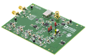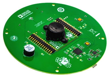
DC2593A
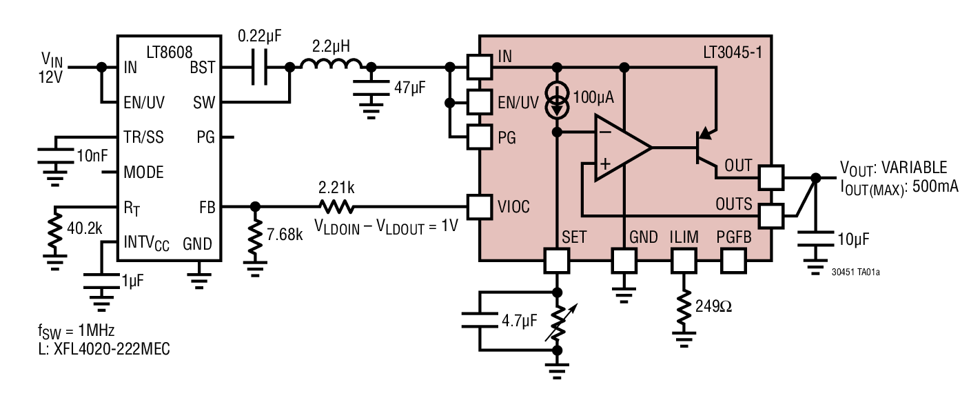
Analog Devices Inc.The LT3045-1 is a high performance low dropout linear regulator featuring LTC?s ultralow noise and ultrahigh PSRR architecture for powering noise sensitive applications. Designed as a precision current reference followed by a high performance voltage buffer, the LT3045-1 can be easily paralleled to further reduce noise, increase output current and spread heat on the PCB. In addition to the LT3045 feature set, the LT3045-1 incorporates a VIOC tracking function to control an upstream switching converter to maintain a constant voltage across the LT3045-1 and hence minimize power dissipation.The device supplies 500mA at a typical 260mV dropout voltage. Operating quiescent current is nominally 2.3mA and drops to

DC2595A
Analog Devices Inc.The LTC3889 is a dual PolyPhase DC/DC synchronous step-down switching regulator controller with I2C-based PMBus compliant serial interface. This controller employs a constant-frequency, current-mode architecture, with high voltage input and output capability along with programmable loop compensation. The LTC3889 is supported by the LTpowerPlay? software development tool with graphical user interface (GUI).The EXTVCC pin supports voltages up to 14V allowing for optimized circuit efficiency and die temperature, and for the controller output to supply the chip power. Switching frequency, output voltage, and device address can be programmed both by digital interface as well as external configuration resistors. Parameters can be set via the digital interface or stored in EEPROM. Both outputs have an independent power good indicator and FAULT function.The LTC3889 can be configured for discontinuous (pulse-skipping) mode or continuous inductor current mode.APPLICATIONS Telecom, Datacom, and Storage Systems Industrial and Point of Load Applications

LT8708 80V VIN and VOUT Synchronous 4-Switch Buck-Boost DC/DC Controller with Flexible Bidirectional Capability
Analog Devices Inc.Demonstration circuit 2596A is a high performance bidirectional buck-boost converter featuring the LT®8708 that can operate from input voltages above, below or equal to the output voltage. The demo board input range is 36V to 75V. The output voltage is set at 48V and the output current limit at 6A.
The controller has integrated input voltage and output voltage regulators and two sets of input and output current regulators that control current flow in forward or reverse direction. Features are included that simplify bidirectional power conversion in battery/capacitor backup systems and other applications that may need regulation of VIN, VOUT, IIN and/or IOUT.
While the current mode control limits the inductor current both in normal and in reverse direction these current limits have some variation as input/output voltage changes. The forward and reverse input and output current regulators offer four accurate current limits that can be set individually.
The input voltage regulator is often used in applications with high impedance power sources and will reduce the forward current if the input voltage drops below the set
point. When operating with reverse current flow the input voltage regulator regulates the voltage at the input side.
The operating mode of the controller is determined through the MODE pin (jumper JP7 Pins 5 to 12) and can be set to discontinuous mode, hybrid discontinuous mode, forced continuous mode and Burst Mode® Operation.
The LT8708 is capable of bidirectional operation when operating in the continuous conduction mode (CCM). DCM, HCM and Burst Mode operation only allow power to flow in one direction. Additional circuitry may be needed depending on the application.
By feeding the LT8708 from a separate low voltage supply the power dissipation can be reduced. The LT8708 will start when >5.5V voltage is applied at the input (VIN pin), and when it is running it will draw current from the EXTVCC pin if the voltage at the pin is > 6.4V.
Typical efficiency with 5A load is above 96.3% across a 36V to 75V input range.
The LT8708 data sheet gives a complete description of the part, operation and application information. The data sheet should be read in conjunction with this quick start guide for DC2596A. The input voltage range of the LT8708 itself is 2.8V (need EXTVCC > 6.4V) to 80V and the output range is 1.3V to 80V.
The LT8708EUHG is assembled in a 40-Lead (5mm × 7mm) plastic QFN package with a thermal pad underneath the chip. Proper board layout is essential for maximum
thermal and electrical performance. See the data sheet Circuit Board Layout Checklist section.

LT8390A Demo Board | VIN = 4V to 24V, (60V Transient) with VOUT = 12V at 4A @ 2MHz
Analog Devices Inc.Demonstration circuit 2598A is a 60V 2MHz synchronous buck-boost controller featuring the LT8390A. It accepts an input voltage from 4V to 24V (with transient to 60V) and regulates 12V output at up to 4A. DC2598A features high efficiency and 2MHz switching frequency, a high speed for a 4-switch buck-boost controller. It has a PGOOD flag, short-circuit fault protection, ISMON current-monitoring output signal, and spread spectrum frequency modulation (SSFM) or frequency synchronization.

Starter Kit for LTC2986-1 | LTC2986-1 Motherboard (DC2618) + 20-Input Breakout Board (DC2210) + Linduino One (DC2026)
Analog Devices Inc.The DC2608 is the starter kit for demonstrating the performance and ease of use of the LTC2986-1, which is a complete temperature measurement system on a chip. This kit includes the DC2618 (main demo circuit containing the LTC2986-1) and the DC2210 (a simple experiment circuit allowing bread boarding). In addition to the starter demonstration kit, sensor specific demonstration boards highlighting the performance of RTDs, thermistors, or thermocouples are also available.

DC2615A
Analog Devices Inc.The LTC7151S is a high efficiency monolithic synchronous buck regulator capable of delivering 15A to the load. It uses a phase lockable controlled on-time constant frequency, current mode architecture. PolyPhase operation allows multiple LTC7151S regulators to run out-of-phase, which reduces the amount of input and output capacitors required. The operating supply voltage range is from 3.1V to 20V.The operating frequency is programmable from 400kHz to 3MHz with an external resistor. The high frequency capability allows the use of physically smaller inductor and capacitor sizes. For switching noise sensitive applications, the LTC7151S can be externally synchronized from 400kHz to 3MHz. The PHMODE pin allows the user control of the phase of the outgoing clock signal. The unique constant frequency/controlled on-time architecture is ideal for high step-down ratio applications that operate at high frequencies while demanding fast transient response. The LTC7151S uses second generation Silent Switcher 2 technology including integrated bypass capacitors to deliver a highly efficient solution at high frequencies with excellent EMI performance.Applications Automotive and Industrial Power Supplies Server Power Applications Distributed Power Systems Point-of-Load Supply for ASIC, FPGA, DSP, ?P, etc.

DC261A-A
Analog Devices Inc.The LT1795 is a dual current feedback amplifier with high output current and excellent large signal characteristics. The combination of high slew rate, 500mA output drive and up to ?15V operation enables the device to deliver significant power at frequencies in the 1MHz to 2MHz range. Short-circuit protection and thermal shutdown insure the device?s ruggedness. The LT1795 is stable with large capacitive loads and can easily supply the large currents required by the capacitive loading. A shutdown feature switches the device into a high impedance, low current mode, reducing power dissipation when the device is not in use. For lower bandwidth applications, the supply current can be reduced with a single external resistor.The LT1795 comes in the very small, thermally enhanced, 20-lead TSSOP package for maximum port density in line driver applications.Applications ADSL HDSL2, G.lite Drivers Buffers Test Equipment Amplifiers Video Amplifiers Cable Drivers

DC2620A-A
Analog Devices Inc.The LTC7106 is a precision, PMBus controlled, bidirectional current digital-to-analog converter that adjusts the output voltage of any conventional VFB referenced regulator. The LTC7106 can work with the vast majority of power management controllers or regulators to enable digital control of the output voltage. Internal power-on reset circuitry keeps the DAC output current at zero (high impedance IDAC) until a valid write takes place. Features include a range bit for easy interfacing to almost any impedance resistor divider, and an open-drain GPO output for controlling the Run or Enable pin of the DC/DC regulator. For most applications, the current DAC error is significantly attenuated with proper design. See more detail about VOUT accuracy in the Applications Information section of this data sheet. The LTC7106 is supported by the ADI LTpowerPlay? development tool with graphical user interface (GUI).Applications General Purpose Power Systems Telecom Systems Industrial Applications

DC2642A-B
Analog Devices Inc.The LTC4041 is a complete supercapacitor backup system for 2.9V to 5.5V supply rails. It contains a high current step-down DC/DC converter to charge a single supercapacitor or two supercapacitors in series. When input power is unavailable, the step-down regulator operates in reverse as a step-up regulator to backup the systemoutput from the supercapacitor(s).The LTC4041?s adjustable input current limit function reduces charge current to protect the input supply from overload while an external disconnect switch isolates theinput supply during backup. When the input supply drops below the adjustable PFI threshold, the 2.5A boost regulator delivers power from the supercapacitor to the systemoutput.An optional input overvoltage protection (OVP) circuit protects the LTC4041 from high voltage damage at the VIN pin. An internal supercapacitor balancing circuit maintainsequal voltages across each supercapacitor and limits the maximum voltage of each supercapacitor to a pre-determined value. The LTC4041 is available in a low profile (0.75mm) 24-Lead 4mm ? 5mm QFN package.ApplicationsRide-Through ?Dying Gasp? SuppliesHigh Current Ride-Through 3V to 5V UPSPower Meters/Industrial AlarmsServers/Solid State Drives

DC2645A
Analog Devices Inc.The LTC5594 is a direct conversion quadrature demodulator optimized for high linearity zero-IF and low-IF receiver applications in the 300MHz to 9GHz frequency range. The very wide IF bandwidth of more than 1GHz makes the LTC5594 particularly suited for demodulation of very wideband signals, especially in 5G front-haul/back-haul receiver applications. The outstanding dynamic range of the LTC5594 makes the device suitable for demanding infrastructure direct conversion applications. Proprietary technology inside the LTC5594 provides the capability to optimize OIP2 to 65dBm, and achieve image rejection better than 60dB. The DC offset control function allows nulling of the DC offset at the A/D converter input, thereby optimizing the dynamic range of true zero-IF receivers that use DC-coupled IF signal paths. The wideband RF and LO input ports make it possible to cover all the major wireless infrastructure frequency bands using a single device. The IF outputs of the LTC5594 are designed to interface directly with most common A/D converter input interfaces. The high OIP3 and high conversion gain of the device eliminate the need for additional amplifiers in the IF signal path.APPLICATIONS 5G Base Station Front-haul/Back-haul Receivers Military and Satellite Receivers Point-to-Point Broadband Radios High Linearity Direct Conversion I/Q SDR Test Instrumentation DPD Receivers

EVAL-AD7887SDZ
Analog Devices Inc.The AD7887 is a high speed, low power, 12-bit analog-to-digital converter (ADC) that operates from a single 2.7 V to 5.25 V power supply. The AD7887 is capable of 125 kSPS throughput rate. The input track-and-hold acquires a signal in 500 ns and features a single-ended sampling scheme. The output coding for the AD7887 is straight binary, and the part is capable of converting full power signals of up to 2.5 MHz.The AD7887 can be configured for either dual- or single-channel operation via the on-chip control register. There is a default single-channel mode that allows the AD7887 to be operated as a read-only ADC. In single-channel operation, there is one analog input (AIN0) and the AIN1/VREF pin assumes its VREF function. This VREF pin allows the user access to the part?s internal 2.5 V reference, or the VREF pin can be overdriven by an external reference to provide the reference voltage for the part. This external reference voltage has a range of 2.5 V to VDD. The analog input range on AIN0 is 0 to VREF.In dual-channel operation, the AIN1/VREF pin assumes its AIN1 function, providing a second analog input channel. In this case, the reference voltage for the part is provided via the VDD pin. As a result, the input voltage range on both the AIN0 and AIN1 inputs is 0 to VDD.CMOS construction ensures low power dissipation of typically 2 mW for normal operation and 3 ?W in power-down mode. The part is available in an 8-lead, 0.15-inch-wide narrow body SOIC and an 8-lead MSOP package.Product HighlightsSmallest 12-bit dual-/single-channel ADC; 8-lead MSOP package.Lowest power 12-bit dual-/single-channel ADC.Flexible power management options, including automatic power-down after conversion.Read-only ADC capability.Analog input range from 0 V to VREF.Versatile serial input/output port (SPI/QSPI/MICROWIRE/ DSP compatible).ApplicationsBattery-powered systems (personal digital assistants, medical instruments, mobile communications)Instrumentation and control systemsHigh speed modems

EVAL-AD7944FMCZ
Analog Devices Inc.The AD7944 is a 14-bit, 2.5 MSPS successive approximation analog-to-digital converter (SAR ADC). It contains a low power, high speed, 14-bit sampling ADC, an internal conversion clock, an internal reference (and buffer), error correction circuits, and a versatile serial interface port. On the rising edge of CNV, the AD7944 samples an analog input, IN+, between 0 V and VREF?with respect to a ground sense, IN?. The AD7944 features avery high sampling rate turbo mode (TURBO high) and areduced power normal mode (TURBO low) for low powerapplications where the power is scaled with the throughput.In normal mode (TURBO low), the SPI-compatible serial interface also features the ability, using the SDI input, to daisy-chainseveral ADCs on a single 3-wire bus and provide an optional busyindicator. The serial interface is compatible with 1.8 V, 2.5 V, and 2.7 V supplies using the separate VIO supply.The AD7944 is available in a 20-lead LFCSP with operationspecified from ?40?C to +85?C.APPLICATIONS Battery-powered equipment Communications ATE Data acquisition systems Medical instruments

EVAL-AD7982SDZ
Analog Devices Inc.The AD7982 is an 18-bit, successive approximation, analog-to-digital converter (ADC) that operates from a single power supply, VDD. The AD7982 contains a low power, high speed, 18-bit sampling ADC and a versatile serial interface port. On the CNV rising edge, the AD7982 samples the voltage difference between the IN+ and IN? pins. The voltages on these pins usually swing in opposite phases between 0 V and VREF. The reference voltage, VREF, is applied externally and can be set independent of the supply voltage, VDD. Its power scales linearly with throughput.The serial peripheral interface (SPI)-compatible serial interface also features the ability, using the SDI input, to daisy-chain several ADCs on a single 3-wire bus and provides an optional busy indicator. The AD7982 is compatible with 1.8 V, 2.5 V, 3 V, and 5 V logic, using the separate VIO supply.The AD7982 is available in a 10-lead MSOP or a 10-lead LFCSP with operation specified from ?40?C to +85?C.Applications Automated test equipment Data acquisition systems Medical instruments Machine automation

EVAL-AD7983SDZ
Analog Devices Inc.The AD7983 is a 16-bit, successive approximation, analog-to-digital converter (ADC) that operates from a single power supply, VDD. It contains a low power, high speed, 16-bit sampling ADC and a versatile serial interface port. On the CNV rising edge, it samples an analog input IN+ between 0 V to REF with respect to a ground sense IN?. The reference voltage, REF, is applied externally and can be set independent of the supply voltage, VDD. Its power scales linearly with throughput.The SPI-compatible serial interface also features the ability, using the SDI input, to daisy-chain several ADCs on a single, 3-wire bus and provides an optional busy indicator. It is compatible with 1.8 V, 2.5 V, 3 V, or 5 V logic, using the separate supply VIO.The AD7983 is housed in a 10-lead MSOP or a 10-lead LFCSP with operation specified from ?40?C to +85?.APPLICATIONS Automated test equipment Data acquisition systems Medical instruments Machine automation

EVAL-AD7991EBZ
Analog Devices Inc.The AD7991 /?AD7995?/?AD7999 are 12-/10-/8-bit, low power, successive approximation ADCs with an I2C?-compatible interface. Each part operates from a single 2.7 V to 5.5 V power supply and features a 1 ?s conversion time. The track-and-hold amplifier allows each part to handle input frequencies of up to 14 MHz, and a multiplexer allows taking samples from four channels.Each AD7991 / AD7995 / AD7999 provides a 2-wire serial interface compatible with I2C interfaces. The AD7991 and AD7995 come in two versions and each version has an individual I2C address. This allows two of the same devices to be connected to the same I2C bus. Both versions support standard, fast, and high speed I2C interface modes. The AD7999 comes in one version.The AD7991 / AD7995 / AD7999 normally remain in a shutdown state, powering up only for conversions. The conversion process is controlled by a command mode, during which each I2C read operation initiates a conversion and returns the result over the I2C bus.When four channels are used as analog inputs, the reference for the part is taken from VDD; this allows the widest dynamic input range to the ADC. Therefore, the analog input range to the ADC is 0 V to VDD;. An external reference, applied through the VIN3/VREF input, can also be used with this part.PRODUCT HIGHLIGHTS Four single-ended analog input channels, or three single-ended analog input channels and one reference input channel. I2C-compatible serial interface. Standard, fast, and high speed modes. Automatic shutdown. Reference derived from the power supply or external reference. 8-lead SOT-23 package.APPLICATIONS System monitoring Battery-powered systems Data acquisition Medical instruments
EVAL-AD7995EBZ
Analog Devices Inc.The AD7991?/ AD7995 /?AD7999 are 12-/10-/8-bit, low power, successive approximation ADCs with an I2C?-compatible interface. Each part operates from a single 2.7 V to 5.5 V power supply and features a 1 ?s conversion time. The track-and-hold amplifier allows each part to handle input frequencies of up to 14 MHz, and a multiplexer allows taking samples from four channels.Each AD7991 / AD7995 / AD7999 provides a 2-wire serial interface compatible with I2C interfaces. The AD7991 and AD7995 come in two versions and each version has an individual I2C address. This allows two of the same devices to be connected to the same I2C bus. Both versions support standard, fast, and high speed I2C interface modes. The AD7999 comes in one version.The AD7991 / AD7995 / AD7999?normally remain in a shutdown state, powering up only for conversions. The conversion process is controlled by a command mode, during which each I2C read operation initiates a conversion and returns the result over the I2C bus.When four channels are used as analog inputs, the reference for the part is taken from VDD; this allows the widest dynamic input range to the ADC. Therefore, the analog input range to the ADC is 0 V to VDD;. An external reference, applied through the VIN3/VREF input, can also be used with this part.PRODUCT HIGHLIGHTS Four single-ended analog input channels, or three single-ended analog input channels and one reference input channel. I2C-compatible serial interface. Standard, fast, and high speed modes. Automatic shutdown. Reference derived from the power supply or external reference. 8-lead SOT-23 packageAPPLICATIONS System monitoring Battery-powered systems Data acquisition Medical instruments

EVAL-AD7998EBZ
Analog Devices Inc.The AD7997?/ AD7998 are 8-channel, 10- and 12-bit, low power,successive approximation ADCs with an I2C-compatibleinterface. The parts operate from a single 2.7 V to 5.5 V powersupply and feature a 2 ?s conversion time. The parts contain an8-channel multiplexer and track-and-hold amplifier that canhandle input frequencies up to 11 MHz.The AD7997 / AD7998 provide a 2-wire serial interface that iscompatible with I2C interfaces. Each part comes in two versions,AD7997-0 / AD7998-0 and AD7997-1 / AD7998-1, and eachversion allows at least two different I2C addresses. The I2C interface on the AD7997-0/AD7998-0 supports standard andfast I2C interface modes. The I2C interface on the AD7997-1 / AD7998-1 supports standard, fast, and high speed I2C interface modes.The AD7997 / AD7998 normally remain in a shutdown statewhile not converting, and power up only for conversions. Theconversion process can be controlled using the CONVST pin,by a command mode where conversions occur across I2C writeoperations or an automatic conversion interval mode selectedthrough software control. The AD7997 / AD7998 require an external reference that shouldbe applied to the REFIN pin and can be in the range of 1.2 V toVDD. This allows the widest dynamic input range to the ADC. On-chip limit registers can be programmed with high andlow limits for the conversion result, and an open-drain, out-of-range indicator output (ALERT) becomes active when theprogrammed high or low limits are violated by the conversionresult. This output can be used as an interrupt.PRODUCT HIGHLIGHTS 2 ?s conversion time with low power consumption. I2C-compatible serial interface with pin-selectable addresses. Two AD7997/AD7998 versions allow five AD7997/AD7998 devices to be connected to the same serial bus. The parts feature automatic shutdown while not converting to maximize power efficiency. Current consumption is 1 ?A max when in shutdown mode at 3V. Reference can be driven up to the power supply. Out-of-range indicator that can be software disabled or enabled. One-shot and automatic conversion rates. Registers store minimum and maximum conversion results.

EVAL-AD8452-4SDZ
Analog Devices Inc.The AD8452 combines a precision analog front-end controller and switch mode power supply (SMPS), pulse-width modulator (PWM) driver into a single silicon platform for high volume battery testing and formation manufacturing. A precision instrumentation amplifier (in-amp) measures the battery charge/discharge current, while an equally accurate difference amplifier measures the battery voltage. Internal laser trimmed resistor networks establish the in-amp and difference amplifier gains (66 V/V and 0.4 V/V, respectively), and stabilize the AD8452 performance across the rated operating temperature range.Desired battery cycling current and voltage levels are established by applying precise control voltages to the ISET and VSET inputs. Actual charge and discharge current levels are sensed (usually by a high power, highly accurate shunt resistor) whose value is carefully selected according to system parameters. Switching between constant current (CC) and constant voltage (CV) loop integration is instantaneous, automatic, and completely transparent to the observer. A logic high at the MODE input selects the charge or discharge mode (high for charge, low for discharge).The AD8452 simplifies designs by providing excellent performance, functionality, and overall reliability in a space saving 48-lead, 7 mm ? 7 mm ? 1.4 mm LQFP package rated for operation at temperatures from ?40?C to +85?C.Applications Battery formation and testing High efficiency battery test systems with recycle capability Battery conditioning (charging and discharging) systems

EVAL-ADA4097-2EBZ
Analog Devices Inc.The ADA4097-1/ADA4097-2 are single and dual robust, precision, rail-to-rail input and output operational amplifiers (op amps) with inputs that operate from ?VS to +VS and beyond, which are referred to in this data sheet as Over-The-Top?. The devices feature offset voltages of ?VS, independent of the +VS supply.The ADA4097-1/ADA4097-2 are unity-gain stable and can drive loads requiring up to 20 mA per channel. The devices can also drive capacitive loads as large as 200 pF. The amplifiers are available with low power shutdown.The ADA4097-1 is available in a standard, 6-lead thin small outline transistor (TSOT) package. The ADA4097-2 is available in an 8-lead standard small outline (SOIC_N) package, 8-lead mini small outline package (MSOP), and 10-lead lead-frame chip-scale package (LFCSP).APPLICATIONS Industrial sensor conditioning Supply current sensing Battery and power supply monitoring Front-end amplifiers in abusive environments 4 mA to 20 mA transmitters

EVAL-ADA4099-1HUJZ
Analog Devices Inc.The ADA4099-1 and ADA4099-2 are single/dual robust, precision, rail-to-rail input/output operational amplifiers (op amps) with inputs that operate from ?VS to +VS and beyond, which is referred to in this data sheet as Over-The-Top?. The devices feature offset voltages of ?VS, independent of the +VS supply.The ADA4099-1 and ADA4099-2 are unity-gain stable and can drive loads requiring up to 20 mA per channel. The device can also drive capacitive loads as large as 100 pF. The amplifiers are available with low power shutdown.The ADA4099-1 is available in a standard, 6-lead, thin small outline transistor (TSOT) package. The ADA4099-2 is available in an 8- lead, standard small outline package (SOIC_N), 8-lead, mini small outline package (MSOP), and a 10-lead, lead frame chip scale package (LFCSP).APPLICATIONS Industrial sensor conditioning Supply current sensing Battery and power supply monitoring Front-end amplifiers in abusive environments 4 mA to 20 mA transmitters