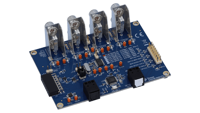
Evaluation Module for UCC25710 LED TV Backlight Controller
Texas InstrumentsEvaluation Module for UCC25710 LED TV Backlight Controller

TPS92602EVM: 2 Channel High Side Current Sense LED Driver Evaluation Module
Texas InstrumentsTPS92602EVM: 2 Channel High Side Current Sense LED Driver Evaluation Module
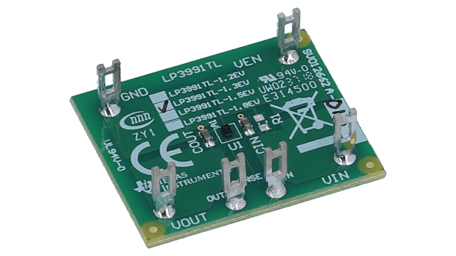
300mA Linear Voltage Regulator for Digital Applications
Texas Instruments300mA Linear Voltage Regulator for Digital Applications
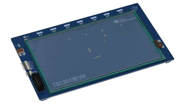
TSC2013-Q1 Evaluation Module for Automotive Resistive Touch Screen Controller
Texas InstrumentsTSC2013-Q1 Evaluation Module for Automotive Resistive Touch Screen Controller
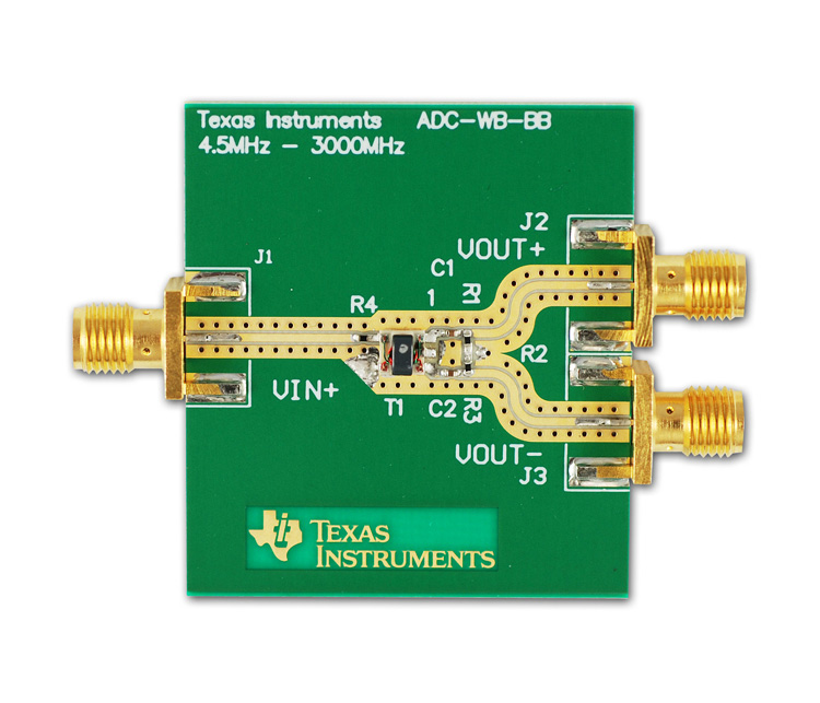
PCM1860 103dB 2-Ch Hardware-Controlled Audio ADC With Universal Front End Evaluation Module
Texas InstrumentsPCM1860 103dB 2-Ch Hardware-Controlled Audio ADC With Universal Front End Evaluation Module
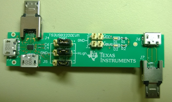
TS3USB3200EVM: USB 2.0 High-Speed and Mobile High-Definition Link Switch Evaluation Module
Texas InstrumentsTS3USB3200EVM: USB 2.0 High-Speed and Mobile High-Definition Link Switch Evaluation Module
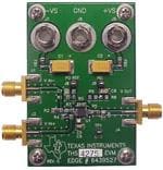
Dual Input, Far Field Noise Suppression Microphone Amplifier
Texas InstrumentsDual Input, Far Field Noise Suppression Microphone Amplifier
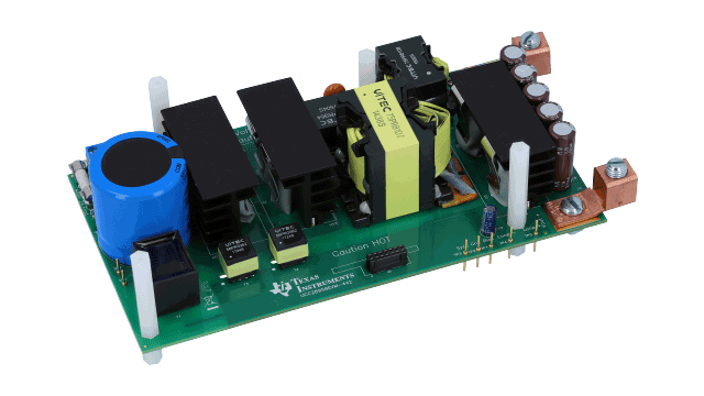
UCC28950 600-W; Phase-Shifted; Full-Bridge Converter Evaluation Module
Texas InstrumentsUCC28950 600-W; Phase-Shifted; Full-Bridge Converter Evaluation Module
3A Fast Response Ultra Low Dropout Linear Regulator
Texas Instruments3A Fast Response Ultra Low Dropout Linear Regulator
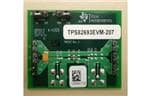
TPS82693 800-mA, High-Efficiency MicroSiP(tm) Step-Down Converter Evaluation Module Board
Texas InstrumentsTPS82693 800-mA, High-Efficiency MicroSiP(tm) Step-Down Converter Evaluation Module Board


