
ADRV9371-N/PCBZ
Analog Devices Inc.The AD9371 is a highly integrated, wideband RF transceiveroffering dual channel transmitters and receivers, integrated synthesizers, and digital signal processing functions. The ICdelivers a versatile combination of high performance and low power consumption required by 3G/4G micro and macro BTSequipment in both FDD and TDD applications. The AD9371operates from 300 MHz to 6000 MHz, covering most of the licensed and unlicensed cellular bands. The IC supports receiver bandwidths up to 100 MHz. It also supports observation receiver and transmit synthesis bandwidths up to 250 MHz to accommodate digital correction algorithms.The transceiver consists of wideband direct conversion signalpaths with state-of-the-art noise figure and linearity. Each complete receiver and transmitter subsystem includes dc offset correction, quadrature error correction (QEC), and programmable digitalfilters, eliminating the need for these functions in the digitalbaseband. Several auxiliary functions such as an auxiliary analog-to-digital converter (ADC), auxiliary digital-to-analog converters (DACs), and general-purpose input/outputs (GPIOs) are integratedto provide additional monitoring and control capability.An observation receiver channel with two inputs is included to monitor each transmitter output and implement interference mitigation and calibration applications. This channel also connects to three sniffer receiver inputs that can monitor radio activity in different bands.The high speed JESD204B interface supports lane rates up to 6144 Mbps. Four lanes are dedicated to the transmitters and four lanes are dedicated to the receiver and observation receiver channels.The fully integrated phase-locked loops (PLLs) provide high performance, low power fractional-N frequency synthesis forthe transmitter, the receiver, the observation receiver, and theclock sections. Careful design and layout techniques provide theisolation demanded in high performance base station applications.All voltage controlled oscillator (VCO) and loop filter components are integrated to minimize the external component count. A 1.3 V supply is required to power the core of the AD9371, anda standard 4-wire serial port controls it. Other voltage supplies provide proper digital interface levels and optimize transmitterand auxiliary converter performance. The AD9371 is packaged in a12 mm ? 12 mm, 196-ball chip scale ball grid array (CSP_BGA).Applications 3G/4G micro and macro base stations (BTS) 3G/4G multicarrier picocells? FDD and TDD active antenna systems? Microwave, nonline of sight (NLOS) backhaul systems

ADUX1020-EVAL-SDP
Analog Devices Inc.The ADUX1020 is a highly efficient photometric sensor with an integrated 14-bit analog-to-digital converter (ADC) and a 20-bit burst accumulator that works in concert with a flexible light emitting diode (LED) driver. It is designed to modulate a LED and measure the corresponding optical return signal. The digital engine includes circuitry and control for data aggregation and proximity detection.The data output and device configuration use a 1.8 V I2C interface. The control circuitry includes flexible LED pulse width and period generation combined with synchronous detection. This circuitry is complemented by a low noise, low power, and wide dynamic range configurable analog front end (AFE), clock generation, LED driver, and digital logic for position and smart sample mode (event driven x, y coordinates, relative z data). This complete AFE features ambient light rejection, avoiding corruption due to external interference.One inexpensive standard surface mount, broad angle or narrow angle IR LED (depending upon application) is required. This LED mounts externally to the ADUX1020.Packaged in a small clear mold 2 mm ? 3 mm, 8-lead LFCSP, the ADUX1020 is specified over an operating temperature range of ?40?C to +85?C.Applications Gesture for user interface (UI )control in portable devices Industrial/automation monitoring Presence detection Angle sensing

ADV3201-EVALZ
Analog Devices Inc.The ADV3200/ADV3201 are 32 ? 32 analog crosspoint switch matrices. They feature a selectable sync-tip clamp input for ac-coupled applications and an on-screen display (OSD) insertion mux. With ?48 dB of crosstalk and ?80 dB isolation at 5 MHz, the ADV3200/ADV3201 are useful in many high density routing applications. The 0.1 dB flatness out to 60 MHz makes the ADV3200/ADV3201 ideal for composite video switching.The 32 independent output buffers of the ADV3200/ADV3201 can be placed into a high impedance state for paralleling crosspoint outputs so that off-channels present minimal loading to an output bus if building a larger array. The part is available in gain of +1 (ADV3200) or +2 (ADV3201) for ease of use in back-terminated load applications. A single 5 V supply, dual ?2.5 V supplies, or dual ?3.3 V supplies (G = +2) can be used while consuming only 250 mA of idle current with all outputs enabled. The channel switching is performed via a double buffered, serial digital control, which can accommodate daisy chaining of several devices.The ADV3200/ADV3201 are packaged in a 176-lead exposed pad LQFP (24 mm ? 24 mm) and are available over the extended industrial temperature range of ?40?C to +85?C.Applications CCTV surveillance Routing of high speed signals including Composite video (NTSC, PAL, S, SECAM) RGB and component video routing Compressed video (MPEG, Wavelet) Video conferencingData Sheet, Rev. 0, 11/2008

ADV3203-EVALZ
Analog Devices Inc.The ADV3202/ADV3203 are 32 ? 16 analog crosspoint switch matrices. They feature a selectable sync-tip clamp input forac-coupled applications and a 2:1 on-screen display (OSD) insertion mux. With ?48 dB of crosstalk and ?80 dB isolationat 5 MHz, the ADV3202/ADV3203 are useful in many high density routing applications. The 0.1 dB flatness out to 60 MHz makes the ADV3202/ADV3203 ideal for both composite and component video switching.The 16 independent output buffers of the ADV3202/ADV3203 can be placed into a high impedance state for paralleling crosspoint outputs so that off-channels present minimal loading to an output bus if building a larger array. The ADV3202 has a gain of +1 while the ADV3203 has a gain of +2 for ease of use in back-terminated load applications. A single +5 V supply, dual ?2.5 V supplies, or dual ?3.3 V supplies can be used while consuming only 195 mA of idle current with all outputs enabled. The channel switching is performed via a double buffered, serial digital control, that can accommodate daisy chaining of several devices.The ADV3202/ADV3203 are packaged in a 176-lead exposed pad LQFP package (24 mm ? 24 mm) and are available over the extended industrial temperature range of ?40?C to +85?C.Applications CCTV surveillance Routing of high speed signals ?Composite video (NTSC, PAL, S, SECAM) ?RGB and component video routing ?Compressed video (MPEG, wavelet) Video conferencingData Sheet, Rev 0, 11/2008

AD2428 MINI Break-Out Board (32-Pin & 100-Pin Connectors)
Analog Devices Inc.ADZS-AD2428MINI is a low-cost, mini break-out board which can interface with EV-SOMCRR-EZKIT (via a 100-pin connector) or any custom board (via a 32 pin 0.1" header). It supports main and subordinate node capability as well as bus and local power configurations.
An Automotive Audio Bus (A2B®) system consists of a single main node and at least one subordinate node, where the transceiver at the host controller is the main node. The main transceiver generates clock, synchronization, and framing for all subordinate nodes and is programmable over a control bus (I2C) for configuration and readback. An extension of this control bus is embedded in the A2B data stream, which enables the host to directly access subordinate transceiver registers and any I2C-connected peripherals on subordinate nodes.
Transceivers can connect directly to PDM microphones and to numerous peripherals via I2C and a multichannel I2S/TDM interface. Finally, the transceiver also supports an A2B bus powering feature, where the main node supplies voltage and current to the subordinate nodes over the same daisy-chained, twisted pair wire cable as used for the communication link, thus eliminating the need for a power supply on bus-powered subordinate nodes. Due to the numerous configurations that are possible for a given A2B system, there are several evaluation platforms that can be used in combination to verify system operation, as summarized in the table below.
Product Comparison Guide
A2B Evaluation Board
Main/Subordinate
Power
Supply
I2S/TDM
PDM Mics
EVAL-AD2428WD1BZ
Main/Subordinate
Local
Yes
3
EVAL-AD2428WB1BZ
Subordinate
Bus
Yes
2
EVAL-AD2428WC1BZ
Subordinate
Bus
No
4
EVAL-AD2428WG1BZ
Subordinate
Local
Yes
0
ADZS-AD2428MINI
Main/Subordinate
Local/Bus
Yes
0
Please contact your local ADI sales office or authorized ADI product distributor to receive additional product information and technical support.

DC048A
Analog Devices Inc.The LTC1066-1 is an 8th order elliptic lowpass filter which simultaneously provides clock-tunability and DC accuracy. The unique and proprietary architecture of the filter allows 14 bits of DC gain linearity and a maximum of 1.5mV DC offset. An external RC is required for DC accurate operation. With ?7.5V supplies, a 20k resistor and a 1?F capacitor, the cutoff frequency can be tuned from 800Hz to 100kHz. A clock-tunable 10Hz to 100kHz operation can also be achieved (see Typical Application section).The filter does not require any external active components such as input/output buffers. The input/output impedance is 500M?/0.1? and the output of the filter can source or sink 40mA. When pin 8 is connected to V+ , the clock-to-cutoff frequency ratio is 50:1 and the input signal is sampled twice per clock cycle to lower the risk of aliasing. For frequencies up to 0.75fCUTOFF , the passband ripple is ?0.15dB. The gain at fCUTOFF is -1dB and the filter?s stopband attenuation is 80dB at 2.3fCUTOFF . Linear phase operation is also available with a clock-to-cutoff frequency ratio of 100:1 when pin 8 is connected to ground.The LTC1066-1 is available in an 18-pin SO Wide package..Applications Instrumentation Data Acquisition Systems Anti-Aliasing Filters Smoothing Filters Audio Signal Processing

LT1372CS8 | 500kHz DC/DC Converter with Shutdown and Synchronous, 5-11VIN, 12VOUT at 250mA
Analog Devices Inc.The LT1372/LT1377 are monolithic high frequency switching regulators. They can be operated in all standard switching configurations including boost, buck, flyback, forward, inverting and 'Cuk.' A 1.5A high efficiency switch is included on the die, along with all oscillator, control and protection circuitry. All functions of the LT1372/LT1377 are integrated into 8-pin SO/PDIP packages.The LT1372/LT1377 typically consumes only 4mA quiescent current and has higher efficiency than previous parts. High frequency switching allows for very small inductors to be used. All surface mount components consume less than 0.5 square inch of board space.New design techniques increase flexibility and maintain ease of use. Switching is easily synchronized to an external logic level source. A logic low on the shutdown pin reduces supply current to 12?A. Unique error amplifier circuitry can regulate positive or negative output voltage while maintaining simple frequency compensation techniques. Nonlinear error amplifier transconductance reduces output overshoot on start-up or overload recovery. Oscillator frequency shifting protects external components during overload conditions.Applications Boost Regulators CCFL Backlight Driver Laptop Computer Supplies Multiple Output Flyback Supplies Inverting Supplies

LTC1174HV-5 | High Efficiency Step-Down DC/DC Converter 5V @ 380mA
Analog Devices Inc.The LTC1174 is a simple current mode DC/DC converter ideally suited for 9V to 5V, 5V to 3.3V or 5V to ?5V operation. With an internal 0.9? switch (at a supply voltage of 9V), the LTC1174 requires only four external components to construct a complete high efficiency DC/DC converter.Under a no load condition the LTC1174 draws only 130?A. In shutdown, it draws a mere 1?A making this converter ideal for current sensitive applications. In dropout, the internal P-channel MOSFET switch is turned on continuously allowing the user to maximize the life of the battery source.The maximum inductor current of the LTC1174 family is pin selectable to either 340mA or 600mA, optimizing efficiency for a wide range of applications. Operation up to 200kHz permits the use of small surface mount inductors and capacitors.For applications requiring higher output current or ultrahigh efficiency, see the LTC1148 data sheet.Applications Distributed Power Systems Step-Down Converters Inverting Converters Memory Backup Supply Portable Instruments Battery-Powered Equipment

LTC1435 | Constant Frequency High Efficiency 3A Converter JPR SEL 1.8V, 2.5V, 2.9V, 3.3V or 5V
Analog Devices Inc.The LTC1435 is a synchronous step-down switching regulator controller that drives external N-channel power MOSFETs using a fixed frequency architecture. Burst Mode? operation provides high efficiency at low load currents. A maximum duty cycle limit of 99% provides low dropout operation which extends operating time in battery-operated systems.The operating frequency is set by an external capacitor allowing maximum flexibility in optimizing efficiency. A secondary winding feedback control pin, SFB, guarantees regulation regardless of load on the main output by forcing continuous operation. Burst Mode operation is inhibited when the SFB pin is pulled low which reduces noise and RF interference.Soft start is provided by an external capacitor which can be used to properly sequence supplies. The operating current level is user-programmable via an external current sense resistor. Wide input supply range allows operation from 3.5V to 30V (36V maximum).For a guaranteed and test minimum on-time refer to the LTC1435A, the 'A' version of the LTC1435. The minimum on-time of the LTC1435A is guaranteed to be ?300ns. The only difference between these two parts is this guaranteed minimum on-time. Pricing is the same.Applications Notebook and Palmtop Computers, PDAs Cellular Telephones and Wireless Modems Portable Instruments Battery-Operated Devices DC Power Distribution Systems

DC1009A-B
Analog Devices Inc.The LTC2488 is a 4-channel (2-channel differential), 16-bit, No Latency ??? ADC with Easy Drive? technology. The patented sampling scheme eliminates dynamic input current errors and the shortcomings of on-chip buffering through automatic cancellation of differential input current. This allows large external source impedances and rail-to-rail input signals to be directly digitized while maintaining exceptional DC accuracy. The LTC2488 includes an integrated oscillator. This device can be configured to measure an external signal from combinations of 4 analog input channels operating in single ended or differential modes. It automatically rejects line frequencies of 50Hz and 60Hz simultaneously. The LTC2488 allows a wide common mode, input range (0V to VCC), independent of the reference voltage. Any combination of single-ended or differential inputs can be selected and the first conversion after a new channel selection is valid.Applications Direct Sensor Digitizer Direct Temperature Measurement Instrumentation Industrial Process Control

LTC2496 | 16-bit, 8-channel ADC, Requires DC590
Analog Devices Inc.DC1011A-B: Demo Board for the LTC2496 16-Bit 8-/16-Channel ΔΣ ADC with Easy Drive Input Current Cancellation.
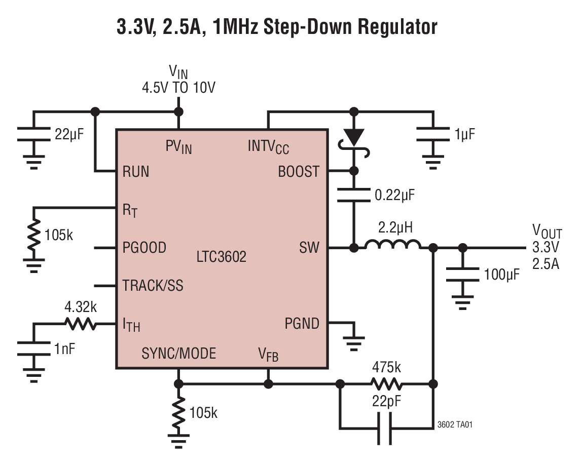
LTC3602EUF | 2.5A, 15V, Monolithic Synchronous Step-Down Regulator
Analog Devices Inc.DC1015A - Demo Board for: LTC3602 - 2.5A, 10V, Monolithic Synchronous Step-Down Regulator

LT3497EDDB Demo Board
Analog Devices Inc.DC1019A - Demo Board for:LT3497 - Dual Full Function White LED Driver with Integrated Schottky Diodes

LTC3210EUD-1 | Main/CAM LED Controller; Requires DC590 Board
Analog Devices Inc.DC1022A: Demo Board for the LTC3210-1 MAIN/CAM LED Controller with 64-Step Brightness Control in 3mm × 3mm QFN

LTC3725EMSE/LTC3726EGN Demo Board | Single-Switch Forward Converter, 36V ≤ VIN ≤ 72V, VOUT = 5V @ 20A
Analog Devices Inc.Demonstration circuit 1031A-C is a 36V-72Vin, synchronous forward converter featuring the LTC3725 forward converter and the LTC3726 secondary-side controller. This circuit was designed specifically to attain a high current, low ripple, synchronously rectified forward converter to efficiently power 5V loads at up to 20A from a typical telecom input voltage range. This circuit features secondary side control of the supply eliminating the need for an optocoupler.

LT3837EFE | 9V to 36V input to 12V at 3A Synchronous Flyback Converter
Analog Devices Inc.Demonstration circuit 1038A-C is a 36W isolated flyback converter with synchronous rectification and primary-side regulation featuring the LT3837. This circuit was designed to demonstrate the high levels of performance, efficiency, and small solution size attainable using the part in a flyback power supply. It operates at 200kHz and produces a regulated 12V, 3A output from an input voltage range of 9V to 36V. Isolation voltage is 1500VDC.
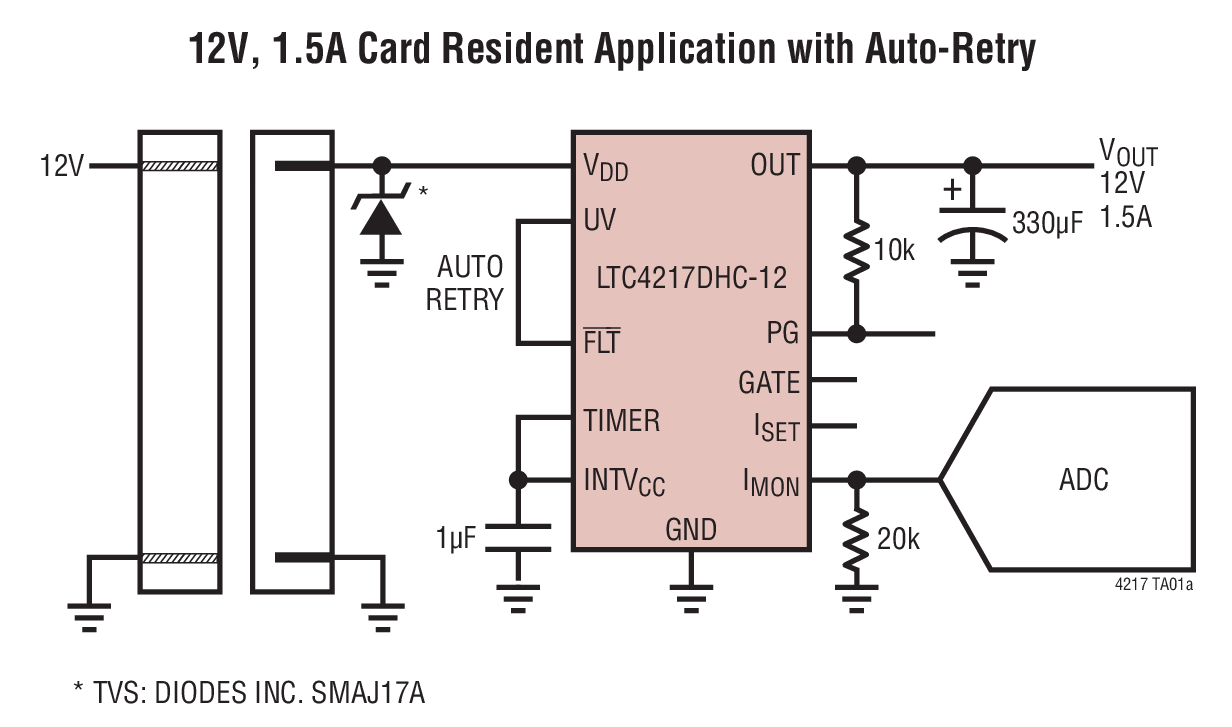
LTC4217 Demo Board | 12V and 24V, 2A Integrated Hot Swap Circuits
Analog Devices Inc.DC1051A: Demo Board for the LTC4217 2A Integrated Hot Swap Controller.

LTC3526LBEDC-2 Demo Board | 2MHz, 0.8V ≤ VIN ≤ 5.5V, VOUT = 1.8V/3.3V/5V @ 100mA
Analog Devices Inc.Demonstration circuits 1053A-E through 1053A-H exercise the LTC3526L family of high efficiency synchronous boost converters, and are capable of operating with an input voltage range from 0.8V to 5.5V. The 2 × 2 mm DFN thermally enhanced package, high switching frequency (1MHz or 2MHz) and 550mA internal power switches provide a very tiny solution. The LTC3526L family also features output disconnect, and the input voltage can be greater or less than the output voltage. DC1053A-G features the LTC3526L-2 (Burst mode operation) and the DC1053A-H features the LTC3526LB-2 (Burst mode defeated). Both have a 2MHz switching frequency and use a 2.2µH inductor.

DC1058A-B
Analog Devices Inc.The LTC2207/LTC2206 are 105Msps/80Msps, sampling 16-bit A/D converters designed for digitizing high frequency, wide dynamic range signals up to input frequencies of 700MHz. The input range of the ADC can be optimized with the PGA front end.The LTC2207/LTC2206 are perfect for demanding communications applications, with AC performance that includes 78.2dB Noise Floor and 100dB spurious free dynamic range (SFDR). Ultralow jitter of 80fsRMS allows undersampling of high input frequencies with excellent noise performance. Maximum DC specs include ?4LSB INL, ?1LSB DNL (no missing codes) over temperature.A separate output power supply allows the CMOS output swing to range from 0.5V to 3.6V.The ENC+ and ENC? inputs may be driven differentially or single-ended with a sine wave, PECL, LVDS, TTL or CMOS inputs. An optional clock duty cycle stabilizer allows high performance at full speed with a wide range of clock duty cycles.? Bits LTC2207-14 14 LTC2207-16 16 Applications Telecommunications Receivers Cellular Base Stations Spectrum Analysis Imaging Systems ATE
DC1058A-D
Analog Devices Inc.The LTC2207/LTC2206 are 105Msps/80Msps, sampling 16-bit A/D converters designed for digitizing high frequency, wide dynamic range signals up to input frequencies of 700MHz. The input range of the ADC can be optimized with the PGA front end.The LTC2207/LTC2206 are perfect for demanding communications applications, with AC performance that includes 78.2dB Noise Floor and 100dB spurious free dynamic range (SFDR). Ultralow jitter of 80fsRMS allows undersampling of high input frequencies with excellent noise performance. Maximum DC specs include ?4LSB INL, ?1LSB DNL (no missing codes) over temperature.A separate output power supply allows the CMOS output swing to range from 0.5V to 3.6V.The ENC+ and ENC? inputs may be driven differentially or single-ended with a sine wave, PECL, LVDS, TTL or CMOS inputs. An optional clock duty cycle stabilizer allows high performance at full speed with a wide range of clock duty cycles.? Bits LTC2207-14 14 LTC2207-16 16 Applications Telecommunications Receivers Cellular Base Stations Spectrum Analysis Imaging Systems ATE


