
EVAL-AD4020FMCZ
Analog Devices Inc.The AD4020 is a high accuracy, high speed, low power, 20-bit, Easy Drive, precision successive approximation register (SAR) analog-to-digital converter (ADC) that operates from a single power supply, VDD. The reference voltage, VREF, is applied externally and can be set independent of the supply voltage. The AD4020 power scales linearly with throughput.Easy Drive features reduce both signal chain complexity and power consumption while enabling higher channel density. The reduced input current, particularly in high-Z mode, coupled with a long signal acquisition phase, eliminates the need for a dedicated ADC driver. Easy Drive broadens the range of companion circuitry that is capable of driving these ADCs (see Figure 2 in the data sheet).Input span compression eliminates the need to provide a negative supply to the ADC driver amplifier while preserving access to the full ADC code range. The input overvoltage clamp protects the ADC inputs against overvoltage events, minimizing disturbances on the reference pin, and eliminating the need for external protection diodes.?Fast device throughput up to 1.8 MSPS allows users to accurately capture high frequency signals and to implement oversampling techniques to alleviate the challenges associated with antialias filter designs. Decreased serial peripheral interface (SPI) clock rate requirements reduce digital input/output power consumption, broadens digital host options, and simplifies the task of sending data across digital isolation. The SPI-compatible serial user interface is compatible with 1.8 V, 2.5 V, 3 V, and 5 V logic by using the separate VIO logic supply.APPLICATIONS Automatic test equipment Machine automation Medical equipment Battery-powered equipment Precision data acquisition systems Instrumentation and control systems

EVAL-AD4030-24-KTZ
Analog Devices Inc.The AD4030-24 is a 2 MSPS successive approximation register (SAR) analog-to-digital converter (ADC) with Easy Drive?. With a guaranteed maximum ?0.9 ppm integral nonlinearity (INL) and no missing codes at 24-bits, the AD4030-24 achieves unparalleled precision from ?40?C to +125?C. Figure 1 in the data sheet shows the functional architecture of the AD4030-24.A low-drift, internal precision reference buffer eases voltage reference sharing with other system circuitry. The AD4030-24 offers a typical dynamic range of 109 dB when using a 5 V reference. The low noise floor enables signal chains requiring less gain and lower power. A block averaging filter with programmable decimation ratio can increase dynamic range up to 155.5 dB. The wide differential input and common mode ranges allow inputs to use the full ?VREF range without saturating, simplifying signal conditioning requirements and system calibration. The improved settling of the Easy Drive analog inputs broadens the selection of analog front-end components compatible with the AD4030-24. Both single-ended and differential signals are supported.The versatile Flexi-SPI serial peripheral interface (SPI) eases host processor and ADC integration. A wide data clocking window, multiple SDO lanes, and optional DDR data clocking can reduce the serial clock to 10 MHz while operating at a sample rate of 2 MSPS. Echo clock mode and ADC host clock mode relax the timing requirements and simplify the use of digital isolators.The BGA package of the AD4030-24 integrates all critical power supply and reference bypass capacitors, reducing the footprint and system component count, and lessening sensitivity to board layout.APPLICATIONS Automatic test equipment Digital control loops Medical instrumentation Seismology Semiconductor manufacturing Scientific instrumentation

DC3160A-A-KIT
Analog Devices Inc.The LTC9101-1/LTC9102/LTC9103 chipset is a 48-port power sourcing equipment (PSE) controller designed for use in IEEE 802.3at Type 2, 802.3bt Type 3 and 4 compliant Power over Ethernet (PoE) systems. The LTC9101-1/LTC9102/LTC9103 is designed to power compliant 802.3af, 802.3at, and 802.3bt PDs. The LTC9101-1/LTC9102/LTC9103 chipset delivers lowest-in-industry heat dissipation by utilizing low-RDS(ON) external MOSFETs and 0.1? sense resistance per power channel. A transformer-isolated communication protocol replaces expensive opto-couplers and complex isolated 3.3V supply, resulting in significant BOM cost savings.Advanced power management features include per-port 14?bit current/power monitoring, programmable current/power limits, and versatile fast shut-down of preselected ports. An advanced power management host software layer is available. PD detection uses a proprietary multipoint detection mechanism ensuring excellent immunity from false PD identification. Autoclass and 5-event physical classification are supported. The LTC9101-1/LTC9102/LTC9103 includes an I2C serial interface operable up to 1MHz. The LTC9101-1/LTC9102/LTC9103 is pin or I2C programmable to negotiate PD delivered power up to 71.3W.APPLICATIONS PoE PSE Switches/Routers and Midspans
DC3160A-B-KIT
Analog Devices Inc.The LTC9101-1/LTC9102/LTC9103 chipset is a 48-port power sourcing equipment (PSE) controller designed for use in IEEE 802.3at Type 2, 802.3bt Type 3 and 4 compliant Power over Ethernet (PoE) systems. The LTC9101-1/LTC9102/LTC9103 is designed to power compliant 802.3af, 802.3at, and 802.3bt PDs. The LTC9101-1/LTC9102/LTC9103 chipset delivers lowest-in-industry heat dissipation by utilizing low-RDS(ON) external MOSFETs and 0.1? sense resistance per power channel. A transformer-isolated communication protocol replaces expensive opto-couplers and complex isolated 3.3V supply, resulting in significant BOM cost savings.Advanced power management features include per-port 14?bit current/power monitoring, programmable current/power limits, and versatile fast shut-down of preselected ports. An advanced power management host software layer is available. PD detection uses a proprietary multipoint detection mechanism ensuring excellent immunity from false PD identification. Autoclass and 5-event physical classification are supported. The LTC9101-1/LTC9102/LTC9103 includes an I2C serial interface operable up to 1MHz. The LTC9101-1/LTC9102/LTC9103 is pin or I2C programmable to negotiate PD delivered power up to 71.3W.APPLICATIONS PoE PSE Switches/Routers and Midspans

DC3219A
Analog Devices Inc.The LT8625S synchronous step-down regulator features third-generation Silent Switcher technology which is uniquely designed to combine an ultralow noise reference with Silent Switcher architecture in order to achieve both high efficiency and excellent wideband noise performance.The innovative ultralow noise architecture provides exceptional low frequency (0.1Hz?100kHz) output noise performance in a switching regulator, independent of output voltage. Silent Switcher architecture minimizes EMI emissions while delivering high efficiency at high switching frequencies.?The LT8625S is ideal for high current, noise sensitive applications which benefit from the high efficiency of a synchronous switching regulator.APPLICATIONS RF Power Suppliers: PLLs, VCOs, Mixers, LNAs, PAs High Speed/High Precision ADCs/DACs Low Noise Instrumentation

DC323A-B
Analog Devices Inc.The LTC1751 family are micropower charge pump DC/DC converters that produce a regulated output voltage at up to 100mA. The input voltage range is 2V to 5.5V. Extremely low operating current (20?A typical with no load) and low external parts count (one flying capacitor and two small bypass capacitors at VIN and VOUT) make them ideally suited for small, battery-powered applications.The LTC1751 family operate as Burst Mode? switched capacitor voltage doublers to achieve ultralow quiescent current. They have thermal shutdown capability and can survive a continuous short circuit from Vout to GND. The PGOOD pin on the LTC1751-3.3 and LTC1751-5 indicates when the output voltage has reached its final value and if the output has an undervoltage fault condition. The FB pin of the adjustable LTC1751 can be used to program the desired output voltage or current. An optional soft-start capacitor may be used at the SS pin to prevent excessive inrush current during start-up.The LTC1751 family is available in an 8-pin MSOP package.Applications Li-Ion Battery Backup Supplies Local 3V and 5V Conversion Smart Card Readers PCMCIA Local 5V Supplies White LED Backlighting

LT5502EGN Demo Board | 400MHz IF Receiver with Limiting Amplifier and I/Q Demodulator
Analog Devices Inc.DC333A-A: Demo Board for the LT5502 400MHz Quadrature IF Demodulator with RSSI.

LTC2420CS8 | 20 Bit Delta Sigma ADC with Turbo Mode (with Diskette, Requires Win95/98)
Analog Devices Inc.DC344A: Demo Board for the LTC2420 20-Bit µPower No Latency Delta-Sigma ADC in SO-8

LTC1928ES6-5 | Low Noise Boost DC/DC Converter, 2.7V to 4.4V Input, 5VOUT @ 30mA
Analog Devices Inc.The LTC1928-5 is a doubler charge pump with an internal low noise, low dropout (LDO) linear regulator. The part is designed to provide a low noise boosted supply voltage for powering noise sensitive devices such as high frequency VCOs in wireless applicationsAn internal charge pump converts a 2.7V to 4.4V input to a boosted output, while the internal LDO regulator converts the boosted voltage to a low noise regulated output. The regulator is capable of supplying up to 30mA of output current. Shutdown reduces the supply current to

LT1725IGN | 48VIN to 5VOUT 2A Module, Isolated Flyback, 1x2 Footprint
Analog Devices Inc.DC373A-A: Demo Board for the LT1725 General Purpose Isolated Flyback Controller.

LTC3716EG | 2-Phase Mobile CPU VRM, 7 to 24VIN, 0.6 to 1.75VOUT @ 25A (maximum performance)
Analog Devices Inc.DC377B-A: Demo Board for the LTC3716 - 2-Phase, 5-Bit VID, Current Mode, High Efficiency, Synchronous Step-Down Switching Regulator
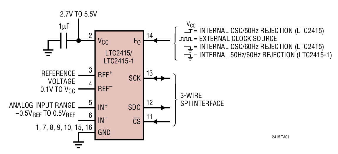
LTC2415CGN | Differential Input 24-Bit ADC with 2X Output Rate (with Diskette, Requires Win95/98)
Analog Devices Inc.DC382A: Demo Board for LTC2415 24-Bit No Latency Delta Sigma ADC with Differential Input and Differential Reference.

LTC3778EF | High Efficiency Notebook CPU Power Supply, Mobile Tualatin, VIN = 7.5V - 24V, VCORE = 1.4V/23Amax + VID
Analog Devices Inc.DC389A-A: Demo Board for LTC3778: Wide Operating Range, No RSENSE Step-Down Controller.

LTC3728EUH Demo Board | Dual Output, 5V to 24VIN, 5VOUT1 @ 4A, 3.3VOUT2 @ 5A
Analog Devices Inc.Demonstration circuit 392 is a dual output, step-down, synchronous buck converter featuring either the 150kHz to 300kHz LTC1628EUH controller (DC392A-A), the 250kHz to 550kHz LTC3728EUH (DC392A-B) or 250kHz to 550kHz LTC3728LUH (DC392A-C). It operates with an input voltage range of 7V to 24V and provides 3.3V @ 5A and 5V @ 4A at its output.

LT1930AES5/LT1931AES5 Demo Board | 3 Circuits: Boost/SEPIC/Inverter: 5VIN to 12VOUT1 @ 250mA, 10V-16VIN to 12VOUT2 @ 250mA, 12VIN to -12VOUT3 @ 250mA
Analog Devices Inc.Demonstration circuit 397 is a multipurpose DC/DC switching regulator using the LT1930A and LT1931A voltage regulators in a SOT-23 package. The demo board offers three separate DC/DC converters for different applications needs. The boost circuit is designed to convert a 5V input to 12V output at 250mA maximum load. The SEPIC circuit generates a constant 12V/250mA (max load) output with a 10V~16V variable input. The inverter circuit is de-signed for applications requiring negative 12V/250mA (max load) from a positive 12V input. All three circuits are designed to demonstrate fast switching frequency (2.2MHz), an internal 36V/1A switch, wide input range, and small circuit size.

LTC3400ES6 | 1.2MHz, High Efficiency Synchronous Boost Converter, VIN = 1V to 3V, VOUT = 3.3V @ 90mA
Analog Devices Inc.DC398A-A: Demo Board for LTC3400 600mA, 1.2MHz Micropower Synchronous Boost Converters in ThinSOT.

LTC3402EMS | Synchronous Boost Converter, VIN=1 to 4.5V, VOUT=3.3V or 5V
Analog Devices Inc.DC409A: Demo Board for the LTC3402 2A, 3MHz Micropower Synchronous Boost Converter

DC413A
Analog Devices Inc.The LTC3404 is a high efficiency monolithic synchronous buck regulator using a constant frequency, current mode architecture. Supply current during operation is only 10?A and drops to < 1?A in shutdown. The 2.65V to 6V input voltage range makes the LTC3404 ideally suited for single Li-Ion battery-powered applications. 100% duty cycle provides low dropout operation, extending battery life in portable systems.Switching frequency is internally set at 1.4MHz, allowing the use of small surface mount inductors and capacitors. For noise sensitive applications the LTC3404 can be externally synchronized from 1MHz to 1.7MHz. Burst Mode operation is inhibited during synchronization or when the SYNC/MODE pin is pulled low, preventing low frequency ripple from interfering with audio circuitry. The internal synchronous switch increases efficiency and eliminates the need for an external Schottky diode. Low output voltages are easily supported with the 0.8V feedback reference voltage. The LTC3404 is available in a space saving 8-lead MSOP package. For higher input voltage (11V abs max) applications, refer to the LTC1877 data sheet.Applications Cellular Telephones Wireless and DSL Modems Personal Information Appliances Portable Instruments Distributed Power Systems Battery-Powered Equipment

LT5511EFE | High Signal Level Up-Converting Mixer (950MHz Output)
Analog Devices Inc.DC426A: Demo Board for the LT5511 High Signal Level Upconverting Mixer.

LTC1967CMS8 | RMS to DC Converter
Analog Devices Inc.DC427B-B: Demo Board for the LTC1967 Precision Extended Bandwidth, RMS-to-DC Converter.


