
EVAL-ADF4150HVEB1Z
Analog Devices Inc.The ADF4150HV is a 3.0 GHz, fractional-N or integer-N frequency synthesizer with an integrated high voltage charge pump. The synthesizer can be used to drive external wideband VCOs directly, eliminating the need for operational amplifiers to achieve higher tuning voltages. This simplifies design and reduces cost while improving phase noise, in contrast to active filter topologies, which tend to degrade phase noise compared to passive filter topologies.The VCO frequency can be divided by 1, 2, 4, 8, or 16 to allow the user to generate RF output frequencies as low as 31.25 MHz. For applications that require isolation, the RF output stage can be muted. The mute function is both pin- and software-controllable.A simple 3-wire interface controls all on-chip registers. The charge pump operates from a power supply ranging from 6 V to 30 V, whereas the rest of the device operates from 3.0 V to 3.6 V. The ADF4150HV can be powered down when not in use.Applications Wireless infrastructure Microwave point-to-point/point-to-multipoint radios VSAT radios Test equipment Private/land mobile radio

EVAL-ADF4151EB1Z
Analog Devices Inc.The ADF4151 allows implementation of fractional-N or integer-N phase-locked loop (PLL) frequency synthesizers if used with an external voltage controlled oscillator (VCO), loop filter, and external reference frequency.The ADF4151 is used with external VCO parts and is footprint and software compatible with the ADF4350. The part consists of a low noise digital phase frequency detector (PFD), a precision charge pump, and a programmable reference divider. There is a ?-? based fractional interpolator to allow programmable fractional-N division. The INT, FRAC, and MOD registers define an overall N divider [N = (INT + (FRAC/MOD))]. The RF output phase is programmable for applications that require a particular phase relationship between the output and the reference. The ADF4151 also features cycle slip reduction circuitry, leading to faster lock times without the need for modifications to the loop filter.Control of all the on-chip registers is through a simple 3-wire interface. The device operates with a power supply ranging from 3.0 V to 3.6 V that can be powered down when not in use.The ADF4151 is available in a 5 mm ? 5 mm package.Applications Wireless infrastructure (W-CDMA, TD-SCDMA, WiMax, GSM, PCS, DCS, DECT) Test equipment Wireless LANs, CATV equipment Clock generation
EVAL-ADF4152HVEB1Z
Analog Devices Inc.The ADF4152HV is a 5.0 GHz, fractional-N or integer N frequency synthesizer with an integrated high voltage charge pump. The synthesizer can drive external wideband voltage controlled oscillators (VCOs) directly, eliminating the need for operational amplifiers to achieve higher tuning voltages. The integrated high voltage charge pump simplifies design and reduces cost while improving phase noise, in contrast to active filter topologies, which tend to degrade phase noise compared to passive filter topologies.The VCO frequency can be divided by 1, 2, 4, 8, or 16 to allow the user to generate RF output frequencies as low as 31.25 MHz. For applications that require isolation, the RF output stage can be muted. The mute function is both pin and software controllable.A simple 3-wire interface controls all on-chip registers. The charge pump operates from a power supply ranging from 6.0 V to 30 V, whereas the rest of the device operates from 3.0 V to 3.6 V. The ADF4152HV can be powered down when not in use.Applications Wireless infrastructure Microwave point to point/point to multipoint radios Very small aperture terminal (VSAT) radios Test equipment Private land mobile radios

EVAL-ADF4154EBZ1
Analog Devices Inc.The ADF4154 is a fractional-N frequency synthesizer that implements local oscillators in the up conversion and down conversion sections of wireless receivers and transmitters. It consists of a low noise digital phase frequency detector (PFD), a precision charge pump, and a programmable reference divider. There is a ?-? based fractional interpolator to allow programmable fractional-N division. The INT, FRAC, and MOD registersdefine an overall N divider (N = (INT + (FRAC/MOD))). In addition, the 4-bit reference counter (R counter) allows selectable REFIN frequencies at the PFD input. A complete phase-locked loop (PLL) can be implemented if the synthesizer is used with an external loop filter and a voltage controlled oscillator (VCO).A key feature of the ADF4154 is the fast-lock mode with a builtintimer. The user can program a predetermined count-down time value so that the PLL will remain in wide bandwidth mode, instead of having to control this time externally.Control of all on-chip registers is via a simple 3-wire interface. The device operates with a power supply ranging from 2.7 V to 3.3 V, and can be powered down when not in use.

EVAL-ADF4350EB2Z
Analog Devices Inc.The ADF4350 allows implementation of fractional-N orinteger-N phase-locked loop (PLL) frequency synthesizersif used with an external loop filter and external referencefrequency.The ADF4350 has an integrated voltage controlled oscillator(VCO) with a fundamental output frequency ranging from2200 MHz to 4400 MHz. In addition, divide-by-1/2/4/8 or 16circuits allow the user to generate RF output frequencies as lowas 137.5 MHz. For applications that require isolation, the RFoutput stage can be muted. The mute function is both pin- andsoftware-controllable. An auxiliary RF output is also available,which can be powered down if not in use.Control of all the on-chip registers is through a simple 3-wireinterface. The device operates with a power supply rangingfrom 3.0 V to 3.6 V and can be powered down when not in use.Applications Wireless infrastructure (W-CDMA, TD-SCDMA, WiMAX, GSM, PCS, DCS, DECT) Test equipment Wireless LANs, CATV equipment Clock generation

EVAL-ADF5001EB2Z
Analog Devices Inc.The ADF5001 prescaler is a low noise, low power, fixed RF divider block that can be used to divide down frequencies as high as 18 GHz to a lower frequency suitable for input into a PLL IC, such as the?ADF4156 or ADF4106. The ADF5001 provides a divide-by-4 function. The ADF5001 operates off a 3.3 V supply and has differential 100 ? RF outputs to allow direct interface to the differential RF inputs of PLLs such as the ADF4156 and ADF4106. ApplicationsPLL frequency range extenderPoint-to-point radios VSAT radios Communications test equipment

EVAL-ADF7012DBZ4
Analog Devices Inc.The ADF7012 is a low power FSK/GFSK/OOK/GOOK/ASK UHF transmitter designed for short-range devices (SRDs). The output power, output channels, deviation frequency, and modulation type are programmable by using four, 32-bit registers.The fractional-N PLL and VCO with external inductor enable the user to select any frequency in the 75 MHz to 1 GHz band. The fast lock times of the fractional-N PLL make the ADF7012 suitable in fast frequency hopping systems. The fine frequency deviations available and PLL phase noise performance facilitates narrow-band operation.There are five selectable modulation schemes: binary frequency shift keying (FSK), Gaussian frequency shift keying (GFSK), binary on-off keying (OOK), Gaussian on-off keying (GOOK), and amplitude shift keying (ASK). In the compensation register, the output can be moved in
EVAL-ADF7012DBZ5
Analog Devices Inc.The ADF7012 is a low power FSK/GFSK/OOK/GOOK/ASK UHF transmitter designed for short-range devices (SRDs). The output power, output channels, deviation frequency, and modulation type are programmable by using four, 32-bit registers.The fractional-N PLL and VCO with external inductor enable the user to select any frequency in the 75 MHz to 1 GHz band. The fast lock times of the fractional-N PLL make the ADF7012 suitable in fast frequency hopping systems. The fine frequency deviations available and PLL phase noise performance facilitates narrow-band operation.There are five selectable modulation schemes: binary frequency shift keying (FSK), Gaussian frequency shift keying (GFSK), binary on-off keying (OOK), Gaussian on-off keying (GOOK), and amplitude shift keying (ASK). In the compensation register, the output can be moved in

EVAL-ADF7021DBZ2
Analog Devices Inc.The ADF7021 is a low power, highly integrated 2FSK/3FSK/4FSK transceiver. It is designed to operate in the narrowband, license-free ISM bands and licensed bands in the 80 MHz to 650 MHz and 862 MHz to 940 MHz frequency ranges. It has both Gaussian and raised cosine data filtering options to improve spectral efficiency for narrowband applications.It is suitable for circuit applications targeted at European ETSI-EN 300-220, the Japanese ARIB STD-T67, the Chinese Short Range Device regulations, and the North American FCC Part 15, Part 90, and Part 95 regulatory standards. A complete transceiver can be built using a small number of external discrete components, making the ADF7021 very suitable for price-sensitive and area-sensitive applications.The transmit section contains a voltage controlled oscillator (VCO) and a low noise fractional-N PLL with output resolution of
EVAL-ADF7021DBZ3
Analog Devices Inc.The ADF7021 is a low power, highly integrated 2FSK/3FSK/4FSK transceiver. It is designed to operate in the narrowband, license-free ISM bands and licensed bands in the 80 MHz to 650 MHz and 862 MHz to 940 MHz frequency ranges. It has both Gaussian and raised cosine data filtering options to improve spectral efficiency for narrowband applications.It is suitable for circuit applications targeted at European ETSI-EN 300-220, the Japanese ARIB STD-T67, the Chinese Short Range Device regulations, and the North American FCC Part 15, Part 90, and Part 95 regulatory standards. A complete transceiver can be built using a small number of external discrete components, making the ADF7021 very suitable for price-sensitive and area-sensitive applications.The transmit section contains a voltage controlled oscillator (VCO) and a low noise fractional-N PLL with output resolution of

EVAL-ADF7021-NDBZ2
Analog Devices Inc.The ADF7021-N is a high performance, low power, narrow-band transceiver based on the ADF7021. The ADF7021-N has IF filter bandwidths of 9 kHz, 13.5 kHz, and 18.5 kHz, making it ideally suited to worldwide narrowband standards and particularly those that stipulate 12.5 kHz channel separation. It is designed to operate in the narrow-band, license-free ISM bands and in the licensed bands with frequency ranges of 80 MHz to 650 MHz and 842 MHz to 916 MHz. The part has both Gaussian and raised cosine transmit data filtering options to improve spectral efficiency for narrow-band applications. It is suitable for circuit applications targeted at the Japanese ARIB STD-T67, the European ETSI EN 300 220, the Korean short range device regulations, the Chinese short range device regulations, and the North American FCC Part 15, Part 90, and Part 95 regulatory standards. A complete transceiver can be built using a small number of external discrete components, making the ADF7021-N very suitable for price-sensitive and area-sensitive applications. The range of on-chip FSK modulation and data filtering options allows users greater flexibility in their choice of modulation schemes while meeting the tight spectral efficiency requirements. The ADF7021-N also supports protocols that dynamically switch among 2FSK, 3FSK, and 4FSK to maximize communica-tion range and data throughput. The transmit section contains two voltage controlled oscillators (VCOs) and a low noise fractional-N PLL with an output resolution of The frequency-agile PLL allows the ADF7021-N to be used in frequency-hopping, spread spectrum (FHSS) systems. Both VCOs operate at twice the fundamental frequency to reduce spurious emissions and frequency pulling problems. The transmitter output power is programmable in 63 steps from ?16 dBm to +13 dBm and has an automatic power ramp control to prevent spectral splatter and help meet regulatory standards. The transceiver RF frequency, channel spacing, and modulation are programmable using a simple 3-wire interface. The device operates with a power supply range of 2.3 V to 3.6 V and can be powered down when not in use. A low IF architecture is used in the receiver (100 kHz), which minimizes power consumption and the external component count yet avoids dc offset and flicker noise at low frequencies. The IF filter has programmable bandwidths of 9 kHz, 13.5 kHz, and 18.5 kHz. The ADF7021-N supports a wide variety of pro-grammable features including Rx linearity, sensitivity, and IF bandwidth, allowing the user to trade off receiver sensitivity and selectivity against current consumption, depending on the application. The receiver also features a patent-pending automatic frequency control (AFC) loop with programmable pull-in range that allows the PLL to track out the frequency error in the incoming signal. The receiver achieves an image rejection performance of 56 dB using a patent-pending IR calibration scheme that does not require the use of an external RF source. An on-chip ADC provides readback of the integrated tempera-ture sensor, external analog input, battery voltage, and RSSI signal, which provides savings on an ADC in some applications. The temperature sensor is accurate to ?10?C over the full oper-ating temperature range of ?40?C to +85?C. This accuracy can be improved by performing a 1-point calibration at room temperature and storing the result in memory.

EVAL-ADF7021-VDB3Z
Analog Devices Inc.The ADF7021-V is a high performance, low power, narrow-band RF transceiver based on the ADF7021-N. The architecture of the ADF7021-V transceiver is similar to that of the ADF7021-N except that an external VCO is used by the on-chip RF synthesizer for applications that require improved phase noise performance.The ADF7021-V is designed to operate in both the license-free ISM bands and in the licensed bands from 80 MHz to 960 MHz.To minimize RF feedthrough and spurious emissions, the external VCO operates at 2? or 4? the desired RF frequency; the ADF7021-V supports a maximum VCO frequency operation of 1920 MHz. The 4? VCO operation is programmable by enabling an additional on-chip divide-by-2 outside the RF synthesizer loop and offers improved phase noise performance.As with the ADF7021-N receiver, the IF filter bandwidths of 9 kHz, 13.5 kHz, and 18.5 kHz are supported, making the ADF7021-V ideally suited to worldwide narrow-band telemetry applications.The part has both Gaussian and raised cosine transmit data filtering options to improve spectral efficiency for narrow-band applications. It is suitable for circuit applications targeted at the following: European ETSI EN 300 220 North American FCC Part 15, Part 90, and Part 95 Japanese ARIB STD-T67 Korean short-range device regulations Chinese short-range device regulationsA complete transceiver can be built using a small number of discrete external components, making the ADF7021-V very suitable for area-sensitive, high performance driven applications.See data sheet for more information.APPLICATIONS Narrow-band, short range device (SRD) standards ETSI EN 300 220 FCC Part 90 (meets Emission Mask D requirements) FCC Part 95 ARIB STD-T67 Wireless Metering Narrow-band wireless telemetry

EVAL-ADF7023-JDB2Z
Analog Devices Inc.The ADF7023-J is a very low power, high performance, highly integrated 2FSK/GFSK/MSK/GMSK transceiver designed for operation in the 902 MHz to 958 MHz frequency band, which covers the ARIB Standard T96 band at 950 MHz. Data rates from 1 kbps to 300 kbps are supported.The transmit RF synthesizer contains a VCO and a low noise fractional-N phase locked loop (PLL) with an output channel frequency resolution of 400 Hz. The VCO operates at twice the fundamental frequency to reduce spurious emissions. The receive and transmit synthesizer bandwidths are automatically, and independently, configured to achieve optimum phase noise, modulation quality, and settling time. The transmitter output power is programmable from ?20 dBm to +13.5 dBm, with automatic PA ramping to meet transient spurious specifications. The part possesses both single-ended and differential PAs, which allow for Tx antenna diversity.The receiver is exceptionally linear, achieving an IP3 specification of ?12.2 dBm and ?11.5 dBm at maximum gain and minimum gain, respectively, and an IP2 specification of 18.5 dBm and 27 dBm at maximum gain and minimum gain, respectively. The receiver achieves an interference blocking specification of 66 dB at a ?2 MHz offset and 74 dB at a ?10 MHz offset. Thus, the part is extremely resilient to the presence of interferers in spectrally noisy environments. The receiver features a novel, high speed, AFC loop, allowing the PLL to find and correct any RF frequency errors in the recovered packet. A patent pending image rejection calibration scheme is available by downloading the image rejection calibration firmware module to program RAM. The algorithm does not require the use of an external RF source nor does it require any user intervention once initiated. The results of the calibration can be stored in nonvolatile memory for use on subsequent power-ups of the transceiver.See data sheet for additional information.Applications Smart metering IEEE 802.15.4g Home automation Process and building control Home Energy Management Systems (HEMS) Wireless sensor networks (WSNs) Wireless healthcare

EVAL-ADF7025DBZ1
Analog Devices Inc.The ADF7025 is a low power, highly integrated FSK transceiver. It is designed for operation in the license?free ISM bands of 433 MHz, 862 MHz to 870 MHz, and 902 MHz to 928 MHz. The ADF7025 can be used for applications operating under the European ETSI EN300-220 or the North American FCC (Part 15) regulatory standards. The ADF7025 is intended for wideband, high data rate applications with deviation frequencies from 100 kHz to 750 kHz and data rates from 9.6 kbps to 384 kbps. A complete transceiver can be built using a small number of external discrete components, making the ADF7025 very suitable for price-sensitive and area-sensitive applications.The ADF7025 transceiver is suitable for operation under FCC 15.247 Digital Modulation Specification characterized by large deviation frequencies. This allows up to 1Watt transmit power without the need to frequency hop, thereby significantly reducing protocol overhead.APPLICATIONS Wireless audio/video Remote control/security systems Wireless metering Keyless entry Home automation

EVAL-ADF7030DB7Z
Analog Devices Inc.The ADF7030 is a low power, high performance, integrated radio transceiver supporting narrowband operation in the 169.4MHz to 169.6MHz ISM bands. The ADF7030 supports transmit and receive operation at 2.4kbps and 4.8kbps using 2GFSK modulation and transmit operation at 6.4kbps using 4GFSK modulation.The ADF7030 features an on-chip ARM? Cortex?-M0 processor that performs radio control and packet management.Applications Wireless M-Bus Mode N (EN 13757-4) Smart metering Social alarms Active tag asset tracking
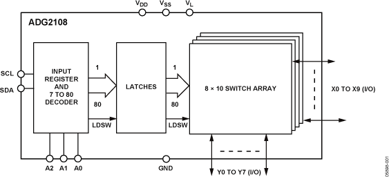
EVAL-ADG2108EBZ
Analog Devices Inc.The ADG2108?is an analog cross point switch with anarray size of 8 ? 10. The switch array is arranged so that there are eight columns by 10 rows, for a total of 80 switchchannels. The array is bidirectional, and the rows and columns can be configured as either inputs or outputs. Each of the 80switches can be addressed and configured through the I2C compatible interface. Standard, full speed, and high speed (3.4 MHz) I2C interfaces are supported. Any simultaneous switch combination is allowed. An additional feature of the ADG2108 is that switches can be updated simultaneously,using the LDSW command. In addition, a RESET option allows all of the switch channels to be reset/off. At power on, all switches are in the off condition. The device is packaged in a 32-lead, 5 mm ? 5 mm LFCSP_VQ.APPLICATIONS AV Switching in TV Automotive Infotainment AV Receivers CCTV Ultrasound Applications KVM Switching Telecom Applications Test Equipment/Instrumentation PBX Systems

EVAL-ADG5421FEBZ
Analog Devices Inc.The ADG5421F is a dual SPST, low on resistance switch that features overvoltage protection, power-off protection, and overvoltage detection on the source pins. When no power supplies are present, the switch remains in the off condition, and the switch inputs are high impedance. When powered, if the analog input signal levels on either of the Sx pins exceed VDD or VSS by the threshold voltage, VT, both switches turn off together, and the open-drain fault flag (FF) pin pulls to a logic low. Input signal levels up to +60 V or ?60 V relative to ground are blocked in both the powered and unpowered condition. The switches turn on with a Logic 1 input and conduct equally well in both directions. The digital input is compatible with 1.8 V logic inputs over the full operating supply range. APPLICATIONS Analog input and output modulesProcess control and distributed control systemsData acquisitionInstrumentationAvionicsAutomatic test equipmentCommunication systemsRelay replacement
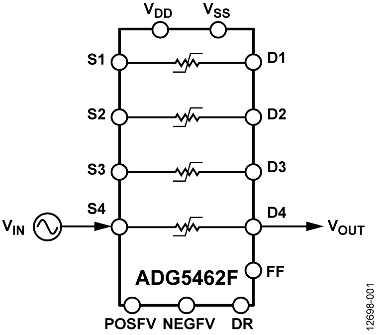
EVAL-ADG5462FEBZ
Analog Devices Inc.The ADG5462F contains four channels that are overvoltage protected. The channel protector is placed in series with the signal path and protects sensitive components from overvoltage faults in that path. The channel protector prevents overvoltages when powered and unpowered, and it is ideal for use in applications where correct power supply sequencing cannot always be guaranteed. The primary supply voltages define the on-resistance profile, while the secondary supply voltages define the voltage level at which the overvoltage protection engages.When no power supplies are present, the channel remains in the off condition, and the channel inputs are high impedance. Under normal operating conditions, if the analog input signal levels on any Sx pin exceed positive fault voltage (POSFV) or negative fault voltage (NEGFV) by a threshold voltage (VT), the channel turns off and that Sx pin becomes high impedance. If the DR pin is driven low, the drain pin (Dx) is pulled to the secondary supply voltage that was exceeded. The output profile for each DR voltage level is shown in Figure 1. Input signal levels up to ?55 V or +55 V relative to ground are blocked in both the powered and unpowered conditions.The low on-resistance of these switches, combined with the on-resistance flatness over a significant portion of the signal range make them an ideal solution for data acquisition and instrumentation applications where excellent linearity and low distortion are critical.Product Highlights Source pins are protected against voltages greater than the secondary supply rails (POSFV and NEGFV), up to ?55 V and +55 V. In an unpowered state, source pins (Sx) are protected against voltages from ?55 V to +55 V. Overvoltage detection with digital output indicates operating state of channel. Trench isolation guards against latch-up. Optimized for low on-resistance and on-resistance flatness. The ADG5462F operates from a dual power supply range of ?5 V to ?22 V or a single power supply range of 8 V to 44 V.Applications Analog input/output modules Process control/distributed control systems Data acquisition Instrumentation Avionics Automatic test equipment Communication systems

EVAL-ADG7421FEBZ
Analog Devices Inc.The ADG7421F is a low voltage, dual single-pole/single-throw (SPST), low on-resistance switch that features overvoltage protection, power-off protection, and overvoltage detection on the source pins.When no power supplies are present, the switch remains in the off condition, and the switch inputs are high impedance. When powered, if the analog input signal levels on the Sx pins exceed VDD or VSS by a threshold voltage, VT, the switch automatically turns off and the digital FF (fault flag) pin drops to a logic low to indicate a fault.Input signal levels up to +60 V or ?60 V relative to ground are blocked, in both the powered and unpowered condition. The switches turn on with a Logic 1 input and conducts equally well in both directions with an analog signal range of VSS + 0.1 V to VDD ? 0.55 V for a 5 V single supply. The digital input is compatible with 1.8 V logic inputs over the full operating supply range.The ADG7421F is ideal for providing overvoltage protection for small signals such as resistance temperature device (RTD) inputs (see Figure 56 in the data sheet) and thermocouple inputs (see Figure 55). The ability to protect against high voltages up to ?60 V coupled with a low voltage supply can enable complete low voltage input stages for industrial applications.APPLICATIONS Analog input/output modules Process control/distributed control systems? Data acquisition? Instrumentation? Avionics? Automatic test equipment? Communication systems Relay replacement

EVAL-ADG884EBZ
Analog Devices Inc.The ADG884 is a low voltage CMOS device containing two independently selectable single-pole, double-throw (SPDT) switches. This device offers ultralow on resistance of 0.41 ? over the full temperature range, making the part an ideal solution for applications that require minimal distortion through the switch. The ADG884 also has the capability of carrying large amounts of current, typically 600 mA at 5 V operation.The ADG884 is available in a 10-ball, 2 mm ? 1.5 mm WLCSP package, a 10-lead LFCSP_WD package, and a 10-lead MSOP package. These tiny packages make the ADG884 the ideal solution for space-constrained applications.When on, each switch conducts equally well in both directions and has an input signal range that extends to the supplies. The ADG884 exhibits break-before-make switching action.Product Highlights Single 1.8 V to 5.5 V operation. High current handling capability (400 mA continuous current). 1.8 V logic compatible. Low THD + N (0.01% typical). Tiny 2 mm ? 1.5 mm WLCSP, 3 mm ? 3 mm 10-lead LFCSP_WD, and 10-lead MSOP packages. ApplicationsCellular phonesPDAsMP3 playersPower routingBattery-powered systemsPCMCIA cardsModemsAudio and video signal routingCommunications systemsData Sheet, Rev. C, 6/08


