
Thin SOT23 1A Load Step-Down DC-DC Regulator Evaluation Module
Texas InstrumentsThin SOT23 1A Load Step-Down DC-DC Regulator Evaluation Module
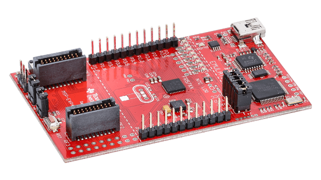
MSP430 Mifare Firmware Development Package
Texas InstrumentsMSP430 Mifare Firmware Development Package
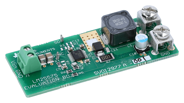
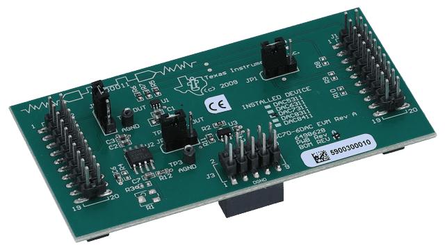
Evaluation Board for LM25575; 42V; 1.5A Step-Down Switching Regulator
Texas InstrumentsEvaluation Board for LM25575; 42V; 1.5A Step-Down Switching Regulator
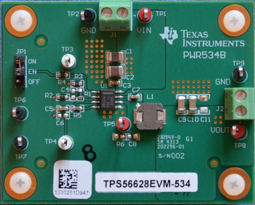
TPS56628EVM-534 - 18V Input; 6-A Synchronous Step Down Converter Evaluation Module
Texas InstrumentsTPS56628EVM-534 - 18V Input; 6-A Synchronous Step Down Converter Evaluation Module
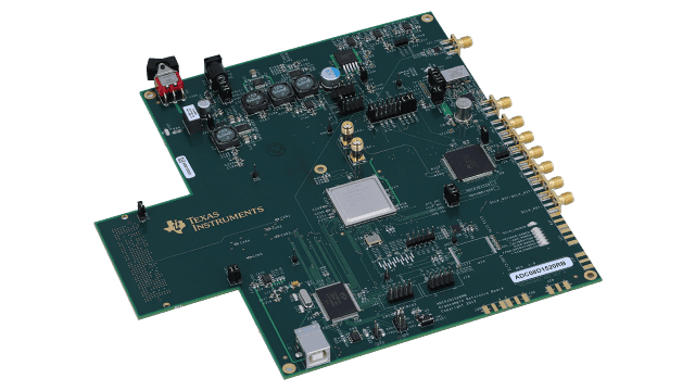
The ADC08D1520RB: Low-Power; 8-Bit; Dual 1.5 GSPS or Single 3.0 GSPS A/D Converter Reference Board
Texas InstrumentsThe ADC08D1520RB: Low-Power; 8-Bit; Dual 1.5 GSPS or Single 3.0 GSPS A/D Converter Reference Board
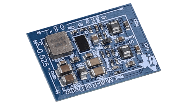
LMR24220 5-Watt Multi-Rail Power Supply Reference Board
Texas InstrumentsLMR24220 5-Watt Multi-Rail Power Supply Reference Board

PCM1864 103dB 4-Ch Software-Controlled Audio ADC With Universal Front End Evaluation Module
Texas InstrumentsPCM1864 103dB 4-Ch Software-Controlled Audio ADC With Universal Front End Evaluation Module
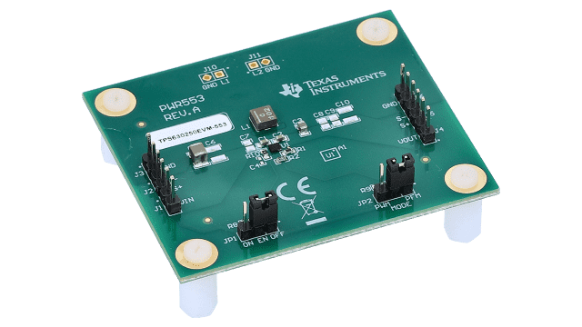
TPS630250 DSBGA evaluation module 4-A switch buck-boost regulator
Texas InstrumentsTPS630250 DSBGA evaluation module 4-A switch buck-boost regulator
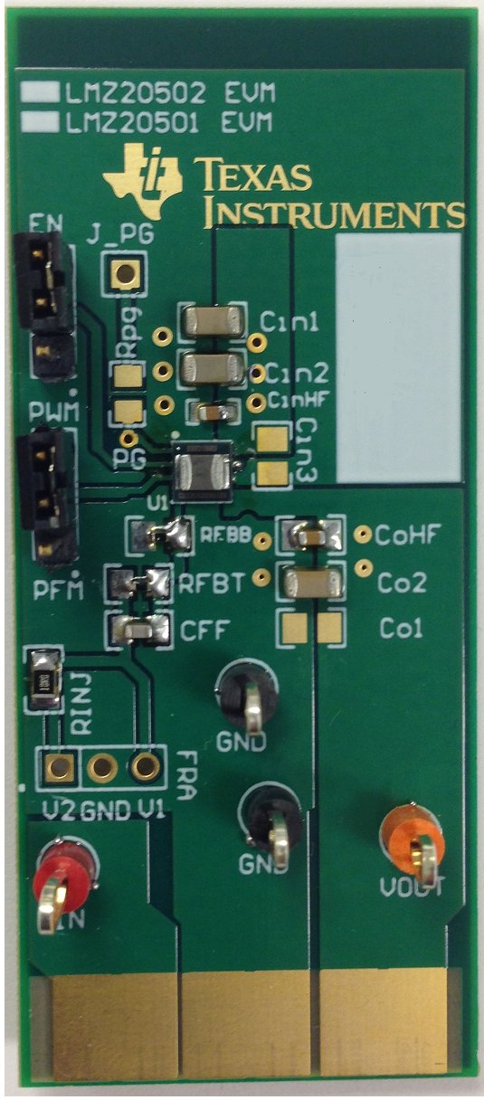
LMZ20502 2A SIMPLE SWITCHER® Nano Module Evaluation Board
Texas InstrumentsLMZ20502 2A SIMPLE SWITCHER® Nano Module Evaluation Board
TPS92210 Evaluation Module for 230VAC TRIAC Dimmable Light Bulb Replacement with Natural PFC
Texas InstrumentsTPS92210 Evaluation Module for 230VAC TRIAC Dimmable Light Bulb Replacement with Natural PFC
Ultra-Low EMI; Filterless; 2.65W; Mono; Class D Audio Power Amplifier (LLP-8)
Texas InstrumentsUltra-Low EMI; Filterless; 2.65W; Mono; Class D Audio Power Amplifier (LLP-8)


