
ADRV9029-HB/PCBZ
Analog Devices Inc.The ADRV9029 is a highly integrated, radio frequency (RF) agile transceiver offering four independently controlled transmitters, dedicated observation receiver inputs for monitoring each transmitter channel, four independently controlled receivers, integrated synthesizers, and digital signal processing functions providing a complete transceiver solution. The device provides the performance demanded by cellular infrastructure applications, such as small cell base station radios, macro 3G/4G/5G systems, and massive multiple in/multiple out (MIMO) base stations.The receiver subsystem consists of four independent, wide bandwidth, direct conversion receivers with wide dynamic range. The four independent transmitters use a direct conversion modulator resulting in low noise operation with low power consumption. The device also includes two wide bandwidth, time shared, observation path receivers with two inputs each for monitoring transmitter outputs.The complete transceiver subsystem includes automatic and manual attenuation control, dc offset correction, quadrature error correction (QEC), and digital filtering, eliminating the need for these functions in the digital baseband. Other auxiliary functions such as analog-to-digital converters (ADCs), digital-to-analog converters (DACs), and general-purpose input/ outputs (GPIOs) that provide an array of digital control options are also integrated.To achieve a high level of RF performance, the transceiver includes five fully integrated phase-locked loops (PLLs). Two PLLs provide low noise and low power fractional-N RF synthesis for the transmitter and receiver signal paths. A third fully integrated PLL supports an independent local oscillator (LO) mode for the observation receiver. The fourth PLL generates the clocks needed for the converters and digital circuits, and a fifth PLL provides the clock for the serial data interface.A multichip synchronization mechanism synchronizes the phase of all LOs and baseband clocks between multiple ADRV9029 chips. All voltage controlled oscillators (VCOs) and loop filter components are integrated and adjustable through the digital control interface.This device contains a fully integrated, low power digital predistortion (DPD) adaptation engine for use in power amplifier linearization. DPD enables use of high efficiency power amplifiers, reducing the power consumption of base station radios while also reducing the number of SERDES lanes necessary to interface with baseband processors.The low power crest factor reduction (CFR) engine of the ADRV9029 reduces the peak to average ratio (PAR) of the input signal, enabling higher efficiency transmit line ups while reducing the processing load on baseband processors.The serial data interface consists of four serializer lanes and four deserializer lanes. The interface supports both the JESD204B and JESD204C standards, operating at data rates up to 24.33 Gbps. The interface also supports interleaved mode for lower bandwidths, thus reducing the number of high speed data interface lanes to one. Both fixed and floating-point data formats are supported. The floating-point format allows internal automatic gain control (AGC) to be invisible to the demodulator device.The ADRV9029 is powered directly from 1.0 V, 1.3 V, and 1.8 V regulators and is controlled via a standard serial peripheral interface (SPI) serial port. Comprehensive power-down modes are included to minimize power consumption in normal use. The ADRV9029 is packaged in a 14 mm ? 14 mm, 289-ball chip scale ball grid array (CSP_BGA).APPLICATIONS3G/4G/5G TDD and FDD massive MIMO, macro and small cell base stations

ADV3200-EVALZ
Analog Devices Inc.The ADV3200/ADV3201 are 32 ? 32 analog crosspoint switch matrices. They feature a selectable sync-tip clamp input forac-coupled applications and an on-screen display (OSD) insertion mux. With ?48 dB of crosstalk and ?80 dB isolationat 5 MHz, the ADV3200/ADV3201 are useful in many high density routing applications. The 0.1 dB flatness out to 60 MHz makes the ADV3200/ADV3201 ideal for composite video switching.The 32 independent output buffers of the ADV3200/ADV3201 can be placed into a high impedance state for paralleling crosspoint outputs so that off-channels present minimal loading to an output bus if building a larger array. The part is available in gain of +1 (ADV3200) or +2 (ADV3201) for ease of use in back-terminated load applications. A single 5 V supply, dual ?2.5 V supplies, or dual ?3.3 V supplies (G = +2) can be used while consuming only 250 mA of idle current with all outputs enabled. The channel switching is performed via a double buffered, serial digital control, which can accommodate daisy chaining of several devices. The ADV3200/ADV3201 are packaged in a 176-lead exposed pad LQFP (24 mm ? 24 mm) and are available over the extended industrial temperature range of ?40?C to +85?C.Applications CCTV surveillance Routing of high speed signals including ????????Composite video (NTSC, PAL, S, SECAM) ????????RGB and component video routing ????????Compressed video (MPEG, Wavelet) Video conferencing?

AMC-ADA4897-1ARZ
Analog Devices Inc.The?ADA4896-2/ADA4897-1 are unity gain stable, low noise, rail-to-rail output, high speed voltage feedback amplifiers that have a quiescent current of 3 mA. With the 1/f noise of 2.4 nV/?Hz at 10 Hz and a spurious-free dynamic range of ?80 dBc at 2 MHz, the ADA4896-2/ADA4897-1 are an ideal solution in a variety of applications, including ultrasound, low noise preamplifiers, and drivers of high performance ADCs. The Analog Devices, Inc., proprietary next generation SiGe bipolar process and innovative architecture enable such high performance amplifiers.TheADA4896-2/ADA4897-1 have 230 MHz bandwidth, 120 V/?s slew rate, and settle to 0.1% in 45 ns. With a wide supply voltage range (3 V to 10 V), the ADA4896-2/ADA4897-1 are ideal candidates for systems that require high dynamic range, precision, and high speed.The ADA4896-2 is available in 8-lead LFCSP and 8-lead MSOP packages. The ADA4897-1 is available in 8-lead SOIC and 6-lead SOT-23 packages. Both the ADA4896-2 and ADA4897-1 work over the extended industrial temperature range of ?40?C to +125?C.Applications Low noise preamplifier Ultrasound amplifiers PLL loop filters High performance ADC drivers DAC buffers

AMC-ADA4940-1ACPZ
Analog Devices Inc.The ADA4940-1 / ADA4940-2 are low noise, low distortion differential amplifiers with very low power consumption. They are an ideal choice for driving low power, high resolution, high performance SAR and sigma-delta (?-?) analog-to-digital converters (ADCs) with resolutions up to 18 bits from dc to 1 MHz on only 1.25 mA of quiescent current. The adjustable level of the output common-mode voltage allows the ADA4940-1/ ADA4940-2 to match the input common-mode voltage of multiple ADCs. The internal common-mode feedback loop provides exceptional output balance, as well as suppression of even-order harmonic distortion products.With the ADA4940-1 / ADA4940-2, differential gain configurations are easily realized with a simple external feedback network of four resistors determining the closed-loop gain of the amplifier. The ADA4940-1 / ADA4940-2 are fabricated using Analog Devices, Inc., complementary bipolar process, enabling them to achieve very low levels of distortion with an input voltage noise of only 3.9 nV/?Hz. The low dc offset and excellent dynamic performance of the ADA4940-1 / ADA4940-2 make them well suited for a variety of data acquisition and signal processing applications.The ADA4940-1 is available in a Pb-free, 3 mm ? 3 mm, 16-lead LFCSP. The ADA4940-2 is available in a Pb-free, 4 mm ? 4 mm, 24-lead LFCSP. The pinout is optimized to facilitate printed circuit board (PCB) layout and minimize distortion. The ADA4940-1 / ADA4940-2 are specified to operate over the ?40?C to +125?C temperature range.Applications Low power ADC drivers Single-ended-to-differential converters Differential buffers Line drivers Medical Imaging Industrial Process Control Portable Electronics

DC052A
Analog Devices Inc.The LTC1410 is a 0.65?s, 1.25Msps, 12-bit sampling A/D converter that draws only 160mW from ?5V supplies. This easy-to-use device includes a high dynamic range sample-and-hold, a precision reference and requires no external components. Two digitally selectable power shutdown modes provide flexibility for low power systems.The LTC1410?s full-scale input range is ?2.5V. Maximum DC specifications include ?1LSB INL and ?1LSB DNL over temperature. Outstanding AC performance includes 71dB S/(N + D) and 82dB THD at the Nyquist input frequency of 625kHz.The unique differential input sample-and-hold can acquire single-ended or differential input signals up to its 20MHz bandwidth. The 60dB common mode rejection allows users to eliminate ground loops and common mode noise by measuring signals differentially from the source.The ADC has a ?P compatible, 12-bit parallel output port. There is no pipeline delay in the conversion results. A separate convert start input and a data ready signal (BUSY) ease connections to FIFOs, DSPs and microprocessors.Applications Telecommunications Digital Signal Processing Multiplexed Data Acquisition Systems High Speed Data Acquisition Spectrum Analysis Imaging Systems

DC059A-C
Analog Devices Inc.The LTC1174 is a simple current mode DC/DC converter ideally suited for 9V to 5V, 5V to 3.3V or 5V to ?5V operation. With an internal 0.9? switch (at a supply voltage of 9V), the LTC1174 requires only four external components to construct a complete high efficiency DC/DC converter.Under a no load condition the LTC1174 draws only 130?A. In shutdown, it draws a mere 1?A making this converter ideal for current sensitive applications. In dropout, the internal P-channel MOSFET switch is turned on continuously allowing the user to maximize the life of the battery source.The maximum inductor current of the LTC1174 family is pin selectable to either 340mA or 600mA, optimizing efficiency for a wide range of applications. Operation up to 200kHz permits the use of small surface mount inductors and capacitors.For applications requiring higher output current or ultrahigh efficiency, see the LTC1148 data sheet.Applications Distributed Power Systems Step-Down Converters Inverting Converters Memory Backup Supply Portable Instruments Battery-Powered Equipment

LTC2489 | 16-Bit 4/2-Channel I2C Easy Drive ΔΣ ADC (Requires DC590B)
Analog Devices Inc.DC1010A-B: Demo Board for the LTC2489 16-Bit 2-/4-Channel ΔΣ ADC with Easy Drive Input Current Cancellation and I2C Interface.

DC1016A-A
Analog Devices Inc.The LT6557 is a high speed triple video ampli?er with an internal ?xed gain of 2 and a programmable DC input bias voltage. This ampli?er features a 400MHz 2VP-P signal bandwidth, 2200V/?s slew rate and a unique ability to drive heavy output loads to 0.8V of the supply rails, making the LT6557 ideal for a single 5V supply, wideband video application. With just one resistor, the inputs of all three ampli?ers can be programmed to a common voltage level, simplifying and reducing the need for external circuitry in the AC-coupled applications. Without the programmable resistor, the input bias circuit becomes inactive, allowing the use of an external clamp circuit or direct coupled input.The LT6557 has separate power supply and ground pins for each ampli?er to improve channel separation and to ease power supply bypassing. The LT6557 provides uncompromised performance in many high speed applications where a low voltage, single supply is required.The LT6557 is available in 16-lead SSOP and 5mm ? 3mm DFN packages.Applications LCD Video Projectors RGB HD Video Ampli?ers Coaxial Cable Drivers Low Supply ADC Drivers

LTC3823EUH Demo Board | 4.5V ≤ VIN ≤ 16V, VOUT = 2.5V @ 10A
Analog Devices Inc.Demonstration circuit 1021A is a high efficiency synchronous step-down DC/DC converter with 4.5V to 16V input range. It can provide 2.5V output with 10A maximum current. The demo board features the LTC3823EUH controller.

DC1028A
Analog Devices Inc.The LT3513 5-output adjustable switching regulator provides power for large TFT-LCD panels. The 38-pin 5mm ? 7mm QFN device can generate a 3.3V or 5V logic supply along with the triple output supply required for the TFT-LCD panel. A lower voltage secondary logic supply may also be generated with the addition of an external NPN driven by the internal linear regulator. A step-down regulator provides a low voltage output, VLOGIC, with up to 1.2A of current while capable of operating from a wide input range of 4.5V to 30V. A high power step-up converter, a lower power step-up converter and an inverting converter provide the three independent output voltages: AVDD, VON and VOFF required by the LCD panel. A high-side PNP provides delayed turn-on of the VON signal and can handle up to 30mA. Protection circuitry ensures that VON is disabled if any of the four outputs are more than 10% below the programmed voltage.Applications Automotive TFT-LCD Displays Large TFT-LCD Desktop Monitors Flat Panel Televisions

DC1031A-A
Analog Devices Inc.The LTC3726 is a secondary-side controller for synchronous forward converters. When used in conjunction with the LTC3705/LTC3725 gate driver and primary-side controllers, the part creates a complete isolated power supply that combines the simplicity of OPTI-LOOP? compensation with the speed of secondary-side control.The LTC3726 has been designed to simplify the design of highly efficient, secondary-side forward converters. Working in concert with the LTC3705 or LTC 3725, the LTC3726 forms a robust, self-starting converter that eliminates the need for the separate bias regulator that is commonly used in secondary-side control applications. In addition, a proprietary scheme is used to multiplex gate drive signals and DC bias power across the isolation barrier through a single, tiny pulse transformer.The LTC3726 is available in a 16-lead SSOP package.Applications Isolated 48V Telecommunication Systems Internet Servers and Routers Distributed Power Step-Down Converters Automotive and Heavy Equipment
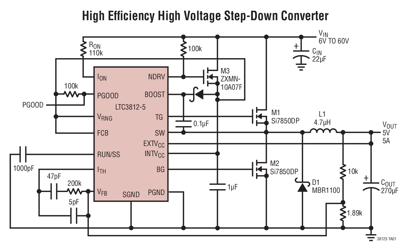
DC1035A
Analog Devices Inc.The LTC3812-5 is a synchronous step-down switching regulator controller that can directly step down voltages from up to 60V input, making it ideal for telecom and automotive applications. The LTC3812-5 uses a constant on-time valley current control architecture to deliver very low duty cycles with accurate cycle-by-cycle current limit without requiring a sense resistor.A precise internal reference provides 0.5% DC accuracy. A high bandwidth (25MHz) error amplifier provides very fast line and load transient response. Large 1? gate drivers allow the LTC3812-5 to drive large power MOSFETs for higher current applications. The operating frequency is selected by an external resistor and is compensated for variations in VIN. A shutdown pin allows the LTC3812-5 to be turned off reducing the supply current to

LT3470EDDB Demo Board | (DFN) 5.5V ≤ VIN ≤ 40V, VOUT = 5V @ 200mA, Integrated Boost and Catch Diodes
Analog Devices Inc.Demonstration circuit 1037 is a 40V micropower DFN buck regulator featuring the LT3470. The board is optimized for 5V output at up to 200mA load current for a steady state input voltage range of 5.5V to 40V. With its wide input voltage range, high efficiency internal power switch, low dropout operation, hysteretic current-mode, integrated boost and catch diodes and tiny SOT-23 package, the LT3470 is a very versatile and powerful IC for DC/DC converters that require extremely compact space, high efficiency and high input voltage.

LT3837EFE | 9V to 36V input to 5V at 7A Synchronous Flyback Converter
Analog Devices Inc.Demonstration circuit 1038A-B is a 35W isolated flyback converter with synchronous rectification and primary-side regulation featuring the LT3837. This circuit was designed to demonstrate the high levels of performance, efficiency, and small solution size attainable using the part in a flyback power supply. It operates at 200kHz and produces a regulated 5V, 7A output from an input voltage range of 9V to 36V. Isolation voltage is 1500VDC.

DC1040A-A
Analog Devices Inc.The LTC3544 is a quad, high efficiency, monolithic synchronous buck regulator using a constant-frequency, current mode architecture. The four regulators operate independently with separate run pins. The 2.25V to 5.5V input voltage range makes the LTC3544 well suited for single Li-Ion/polymer battery-powered applications. 100% duty cycle provides low dropout operation, extending battery runtime in portable systems. Low ripple Burst Mode? operation increases efficiency at light loads, further extending battery runtime with typically only 20mV of ripple.Switching frequency is internally set to 2.25MHz, allowing the use of small surface mount inductors and capacitors. The internal synchronous switches increase efficiency and eliminate the need for external Schottky diodes. Low output voltages are easily supported with the 0.8V feedback reference voltage.The LTC3544 is available in a low profile (0.75mm) (3mm ? 3mm) QFN package. Light Load Operation LTC3544 Burst Mode (20mVP-P),

LTC3544BEUD Demo Board
Analog Devices Inc.DC1040A-B: Demo Board for the LTC3544B Quad Synchronous Step-Down Regulator, 2.25MHz, 300mA, 200mA, 200mA and 100mA.

LTC3780EG/LTC4440ES6 Demo Board | Buck-Boost, VIN: 36V to 72V, VOUT 48V/5A
Analog Devices Inc.Demonstration circuit 1046A is a non-isolated, high efficiency buck-boost DC/DC supply featuring LTC3780EG and LTC4440ES6. The LTC3780 is a high performance 4-switch synchronous buck boost regulator and the LTC4440 is a 100V-rated FET driver. The input voltage of the demo board is designed for 36V to 72V. The output voltage is 48V. At 25C° room temperature, the maximum output current is 5A without a cooling fan and 6A with 150LFM air flow for cooling. An optional 12V bias flyback supply using the LTC3803 is stuffed on the board to power the LTC3780 and LTC4440.

DC104B-C
Analog Devices Inc.The LTC1068 product family consists of four monolithic clock-tunable filter building blocks. Each product contains four matched, low noise, high accuracy 2nd order switched-capacitor filter sections. An external clock tunes the center frequency of each 2nd order filter section. The LTC1068 products differ only in their clock-to-center frequency ratio. The clock-to-center frequency ratio is set to 200:1 (LTC1068-200), 100:1 (LTC1068), 50:1 (LTC1068-50) or 25:1 (LTC1068-25). External resistors can modify the clock-to-center frequency ratio. High performance, quad 2nd order, dual 4th order or 8th order filters can be designed with an LTC1068 family product. Designing filters with an LTC1068 product is fully supported by FilterCAD? filter design software for Windows. The LTC1068 products are available in a 28-pin SSOP surface mount package. A customized version of an LTC1068 family product can be obtained in a 16-lead SO package with internal thin-film resistors. Please contact LTC Marketing for details.Applications Lowpass or Highpass Filters: LTC1068-200, 0.5Hz to 25kHz; LTC1068, 1Hz to 50kHz; LTC1068-50, 2Hz to 50kHz; LTC1068-25, 4Hz to 200kHz Bandpass or Bandreject (Notch) Filters: LTC1068-200, 0.5Hz to 15kHz; LTC1068, 1Hz to 30kHz; LTC1068-50, 2Hz to 30kHz; LTC1068-25, 4Hz to 140kHz

DC1052A-A
Analog Devices Inc.The LTC4218 is a Hot Swap?controller that allows a board to be safely inserted and removed from a live backplane. An internal high side switch driver controls the gate of an external N-channel MOSFET for supply voltages from 2.9V to 26.5V. A dedicated 12V version (LTC4218-12) contains preset 12V specific thresholds, while the standard LTC4218 allows adjustable thresholds.The LTC4218 provides an accurate (5%) current limit with current foldback limiting. The current limit threshold can be adjusted dynamically using an external pin. Additional features include a current monitor output that amplifies the sense voltage for ground referenced current sensing. Overvoltage, undervoltage and power good monitoring are also provided.Applications RAID Systems ATCA, AMC, ?TCA Systems Server I/O Cards Industrial

LTC3526LBEDC Demo Board | 1MHz, 0.8V ≤ VIN ≤ 5.5V, VOUT = 1.8V/3.3V/5V @ 100mA
Analog Devices Inc.Demonstration circuits 1053A-E through 1053A-H exercise the LTC3526L family of high efficiency synchronous boost converters, and are capable of operating with an input voltage range from 0.8V to 5.5V. The 2 × 2 mm DFN thermally enhanced package, high switching frequency (1MHz or 2MHz) and 550mA internal power switches provide a very tiny solution. The LTC3526L family also features output disconnect, and the input voltage can be greater or less than the output voltage. DC1053A-E features the LTC3526L (Burst mode operation) and the DC1053A-F features the LTC3526LB (Burst mode defeated). Both have a 1MHz switching frequency and use a 4.7µH inductor.


