
131997-HMC837LP6CE
Analog Devices Inc.The HMC837LP6CE is a fully functioned Fractional-N Phase-Locked-Loop (PLL) Frequency Synthesizer with an Integrated Voltage Controlled Oscillator (VCO). The synthesizer consists of an integrated low noise VCO with a triband output, an autocalibration subsystem for low voltage VCO tuning, a very low noise digital Phase Detector (PD), a precision controlled charge pump, a low noise reference path divider and a fractional divider.The fractional synthesizer features an advanced delta-sigma modulator design that allows both ultra-fine step sizes and low spurious products. The phase detector (PD) features cycle slip prevention (CSP) technology to allow faster frequency hopping times. Ultra low in-close phase noise and low spurious also allows wider loop bandwidths for faster frequency hopping and low micro-phonics.For theory of operation and register map refer to the 'PLLs with Integrated VCO - RF VCOs' Operating Guide.Applications Cellular/4G Infrastructure Repeaters & Femtocells Communications?Test Equipment CATV Equipment Phased Array Applications DDS Replacement? Very High Data Rate Radios

AD604-EVALZ
Analog Devices Inc.The AD604 is an ultralow noise, very accurate, dual-channel, linear-in-dB variable gain amplifier (VGA) optimized for time-based variable gain control in ultrasound applications; however, it supports any application requiring low noise, wide bandwidth, variable gain control. Each channel of the AD604 provides a 300 k? input resistance and unipolar gain control for ease of use. User determined gain ranges, gain scaling (dB/V), and dc level shifting of output further optimize performance.Each channel of the AD604 utilizes a high performance preamplifier that provides an input referred noise voltage of 0.8 nV/?Hz. The very accurate linear-in-dB response of the AD604 is achieved with the differential input exponential amplifier (DSX-AMP) architecture. Each of the DSX-AMPs comprise a variable attenuator of 0 dB to 48.36 dB followed by a high speed fixed gain amplifier. The attenuator is a 7-stage R-1.5R ladder network. The attenuation between tap points is 6.908 dB and 48.36 dB for the ladder network.The equation for the linear-in-dB gain response isG(dB) = (Gain Scaling?(dB/V) נVGN?(V))+ (Preamp Gain?(dB) ? 19 dB)Preamplifier gains between 5 and 10 (14 dB and 20 dB) provide overall gain ranges per channel of 0 dB through 48 dB and 6 dB through 54 dB. The two channels of the AD604 can be cascaded to provide greater levels of gain range by bypassing the second channel?s preamplifier. However, in multiple channel systems, cascading the AD604 with other devices in the AD60x VGA family that do not include a preamplifier may provide a more efficient solution. The AD604 provides access to the output of the preamplifier, allowing for external filtering between the preamplifier and the differential attenuator stage.Note that scale factors up to 40 dB/V are achievable with reduced accuracy for scales above 30 dB/V. The gain scales linearly-in-dB with control voltages of 0.4 V to 2.4 V with the 20 dB/V scale. Below and above this gain control range, the gain begins to deviate from the ideal linear-in-dB control law. The gain control region below 0.1 V is not used for gain control. In fact when the gain control voltage is

AD605-EVALZ
Analog Devices Inc.The AD605 is a low noise, accurate, dual-channel, linear-in-dB variable gain amplifier (VGA), optimized for any application requiring high performance, wide bandwidth variable gain control. Operating from a single 5 V supply, the AD605 provides differential inputs and unipolar gain control for ease of use. Added flexibility is achieved with a user-determined gain range and an external reference input that provide user-determined gain scaling (dB/V). The high performance linear-in-dB response of the AD605 is achieved with the differential input, single-supply, exponential amplifier (DSX-AMP) architecture. Each of the DSX-AMPs comprises a variable attenuator of 0 dB to ?48.4 dB followed by a high speed, fixed-gain amplifier. The attenuator is based on a 7-stage R-1.5R ladder network. The attenuation between tap points is 6.908 dB, and 48.360 dB for the entire ladder network. The DSX-AMP architecture results in 1.8 nV/?Hz input noise spectral density and accepts a ?2.0 V input signal when VOCM is biased at VP/2. Each independent channel of the AD605 provides a gain range of 48 dB that can be optimized for the application. Gain ranges between ?14 dB to +34 dB and 0 dB to +48 dB can be selected by a single resistor between Pin FBK and Pin OUT. The lower and upper gain ranges are determined by shorting Pin FBK to Pin OUT or leaving Pin FBK unconnected, respectively. The two channels of the AD605 can be cascaded to provide 96 dB of very accurate gain range in a monolithic package. The gain control interface provides an input resistance of approximately 2 M? and scale factors from 20 dB/V to 30 dB/V for a VREF input voltage of 2.5 V to 1.67 V, respectively. Note that scale factors up to 40 dB/V are achievable with reduced accuracy for scales above 30 dB/V. The gain scales linearly in dB with control voltages (VGN) of 0.4 V to 2.4 V for the 20 dB/V scale and 0.20 V to 1.20 V for the 40 dB/V scale. When VGN is The AD605 is available in a 16-lead PDIP and a 16-lead SOIC_N package and is guaranteed for operation over the ?40?C to +85?C temperature range. ApplicationsUltrasound and sonar time-gain controls High performance AGC systems Signal measurement Data Sheet, Rev. E, 5/07

AD6649EBZ
Analog Devices Inc.The AD6649 is a mixed-signal intermediate frequency (IF) receiverconsisting of dual 14-bit, 250 MSPS ADCs and a wideband digitaldownconverter (DDC) and a bypass-able sample rate converter (SRC). The AD6649 is designed to support communications applications where low cost, small size, wide bandwidth and versatility are desired.The dual ADC core features a multistage, differential pipelinedarchitecture with integrated output error correction logic. Each ADC features wide bandwidth inputs supporting a variety of user-selectable input ranges. An integrated voltage reference eases design considerations. A duty cycle stabilizer is provided to compensate for variations in the ADC clock duty cycle, allowing the converters to maintain excellent performance.ADC data outputs are internally connected directly to the digitaldownconverter (DDC) of the receiver. The digital receiver has two channels and provides processing flexibility. Each receive channel has four cascaded signal processing stages: a 32-bit frequency translator (numerically controlled oscillator (NCO), an optional sample rate converter, a fixed FIR filter, and an fs/4 fixed-frequency NCO.In addition to the receiver DDC, the AD6649 has several functions that simplify the automatic gain control (AGC) function in the system receiver. The programmable threshold detector allows monitoring of the incoming signal power using the fast detect output bits of the ADC. If the input signal level exceeds the programmable threshold, the fast detect indicator goes high. Because this threshold indicator has low latency, the user can quickly turn down the system gain to avoid an overrange condition at the ADC input.After digital processing, data is routed directly to the 14-bit output port. These outputs operate at 1.8 V LVDS signal levels.The AD6649 receiver digitizes a wide spectrum of IF frequencies.Each receiver is designed for simultaneous reception of the main channel and the diversity channel. This IF sampling architecture greatly reduces component cost and complexity compared with traditional analog techniques or less integrated digital methods. In diversity applications the output data format is real due to the final NCO which shifts the output center frequency to fs/4.Flexible power-down options allow significant power savings,when desired.Programming for setup and control is accomplished using a 3-pinSPI-compatible serial interface.The AD6649 is available in a 64-lead LFCSP and is specified overthe industrial temperature range of ?40?C to +85?C.APPLICATIONS Communications Diversity radio systems Multimode digital receivers (3G) TD-SCDMA, WiMax, WCDMA, CDMA2000, GSM, EDGE, LTE General-purpose software radios Broadband data applicationsPRODUCT HIGHLIGHTS Integrated dual, 14-bit, 250 MSPS ADC. Integrated wideband decimation filter and 32-bit complex NCO. Fast overrange and threshold detect. Proprietary differential input maintains excellent SNR performance for input frequencies up to 300 MHz. SYNC input allows synchronization of multiple devices. 3-pin, 1.8V SPI port for register programming and register readback.

AD6674-500EBZ
Analog Devices Inc.The AD6674 is a 385 MHz bandwidth mixed-signal intermediate frequency (IF) receiver. It consists of two, 14-bit 1.0 GSPS/750 MSPS/500 MSPS analog-to-digital converters (ADC) and various digital signal processing blocks consisting of four wideband DDCs, an NSR, and VDR monitoring. It has an on-chip buffer and a sample-and-hold circuit designed for low power, small size, and ease of use. This product is designed to support communications applications capable of sampling wide bandwidth analog signals of up to 2 GHz. The AD6674 is optimized for wide input bandwidth, high sampling rate, excellent linearity, and low power in a small package.The dual ADC cores feature a multistage, differential pipelined architecture with integrated output error correction logic. Each ADC features wide bandwidth inputs supporting a variety of user-selectable input ranges. An integrated voltage reference eases design considerations.Applications Diversity multiband, multimode digital receivers 3G/4G, TD-SCDMA, W-CDMA, GSM, LTE, LTE-A DOCSIS 3.0 CMTS upstream receive paths HFC digital reverse path receivers
AD6674-LF750EBZ
Analog Devices Inc.The AD6674 is a 385 MHz bandwidth mixed-signal intermediate frequency (IF) receiver. It consists of two, 14-bit 1.0 GSPS/750 MSPS/500 MSPS analog-to-digital converters (ADC) and various digital signal processing blocks consisting of four wideband DDCs, an NSR, and VDR monitoring. It has an on-chip buffer and a sample-and-hold circuit designed for low power, small size, and ease of use. This product is designed to support communications applications capable of sampling wide bandwidth analog signals of up to 2 GHz. The AD6674 is optimized for wide input bandwidth, high sampling rate, excellent linearity, and low power in a small package.The dual ADC cores feature a multistage, differential pipelined architecture with integrated output error correction logic. Each ADC features wide bandwidth inputs supporting a variety of user-selectable input ranges. An integrated voltage reference eases design considerations.Applications Diversity multiband, multimode digital receivers 3G/4G, TD-SCDMA, W-CDMA, GSM, LTE, LTE-A DOCSIS 3.0 CMTS upstream receive paths HFC digital reverse path receivers

AD6679-500EBZ
Analog Devices Inc.The AD6679 is a 135 MHz bandwidth mixed-signal intermediate frequency (IF) receiver. It consists of two, 14-bit, 500 MSPS analog-to-digital converters (ADCs) and various digital signal processing blocks consisting of four wideband DDCs, an NSR, and VDR monitoring. It has an on-chip buffer and a sample-and-hold circuit designed for low power, small size, and ease of use. This product is designed to support communications applications capable of sampling wide bandwidth analog signals of up to 2 GHz. The AD6679 is optimized for wide input bandwidth, high sampling rates, excellent linearity, and low power in a small package.The dual ADC cores feature a multistage, differential pipelined architecture with integrated output error correction logic. Each ADC features wide bandwidth inputs supporting a variety of user-selectable input ranges. An integrated voltage reference eases design considerations.Applications Diversity multiband, multimode digital receivers 3G/4G, TD-SCDMA, W-CDMA, GSM, LTE, LTE-A? DOCSIS 3.0 CMTS upstream receive paths? HFC digital reverse path receivers?

AD8034ART-EBZ
Analog Devices Inc.FastFETs are an entirely new class of amplifiers from Analog Devices, of which the AD8034 and AD8065 are the first two parts to be released. FastFETs combine the desirable specs of FET input amps (high input impedance that almost eliminates the need to consider the input bias current in designs) with those of ADI's proprietary XFCB technology (most especially low power consumption, low noise and distortions, and a wide supply voltage). We believe FastFETs?will change the way designers think about amplifiers in general, and FET amps specifically.Certainly any designers currently using FETs will certainly be interested in a high-performance and high-speed FET amp that uses a fraction of the power, in packages as small as SC-70.AD8033 (Single amp) SOIC-8 and SC70AD8034 (Dual amp) SOIC-8 and SOT23-8

AD8054ARU-EBZ
Analog Devices Inc.The AD8051 (single), AD8052 (dual) and AD8054 (quad) arelow cost, high speed, voltage feedback amplifiers. The amplifiers operate on +3 V, +5 V or ?5 V supplies at low supply current. They have true single-supply capability with an input voltage range extending 200 mV below the negative rail and within 1 V of the positive rail.Despite their low cost, the AD8051/AD8052/AD8054 provideexcellent overall performance and versatility. The output voltageswings to within 25 mV of each rail, providing themaximum output dynamic range with excellent overdrive recovery.The AD8051/AD8052/AD8054 are well suited for video electronics, cameras, video switchers, or any high speed portable equipment. Low distortion and fast settling make them ideal for active filter applications.The AD8051/AD8052 in the 8-lead SOIC, the AD8052 in the MSOP, the AD8054 in the 14-lead SOIC, and the 14-lead TSSOP packages are available in the extended temperature range of ?40?C to +125?C.ApplicationsActive filtersAnalog-to-digital driversClock bufferConsumer videoProfessional camerasCCD imaging systemsCD/DVD ROMs

AD8074Z-EVAL
Analog Devices Inc.The AD8074 /AD8075 are high-speed triple video buffers with a G = +1 and +2 respectively. They operate on ?5V and have a -3dB full signal bandwidth in excess of 500MHz, along with slew rates in excess of 1350V/?s. With better than -80dB of all hostile crosstalk and 90dB isolation, they are useful in many high-speed applications. The differential gain and differential phase error are 0.01% and 0.01?. Gain Flatness of 0.1dB up to 70MHz make the AD8074/75 ideal for RGB buffering or driving. They consume less than 30mA on a ?5V supply voltage.??Both devices offer a high-speed disable feature that allows the outputs to be put into a high impedance state. This allows the building of larger input arrays while minimizing 'OFF' channel output loading. The AD8074/75 are offered in a 16 lead TSSOP package.

AD8130ARM-EBZ
Analog Devices Inc.The AD8129/AD8130 are designed as receivers for the transmission of high speed signals over twisted-pair cables to work with the AD8131 or AD8132 drivers. Either can be used for analog or digital video signals and for high speed data transmission. The AD8129/AD8130 are differential-to-single-ended amplifiers with extremely high CMRR at high frequency. Therefore, they canalso be effectively used as high speed instrumentation amps or for converting differential signals to single-ended signals.The AD8129 is a low noise, high gain (10 or greater) version intended for applications over very long cables, where signal attenuation is significant. The AD8130 is stable at a gain of 1 and can be used for applications where lower gains are required. Both have user-adjustable gain to help compensate for losses in the transmission line. The gain is set by the ratio of two resistor values. The AD8129/AD8130 have very high input impedance on both inputs, regardless of the gain setting. The AD8129/AD8130 have excellent common-mode rejection (70 dB @ 10 MHz), allowing the use of low cost, unshielded twisted-pair cables without fear of corruption by external noise sources or crosstalk. The AD8129/AD8130 have a wide power supply range from single +5 V to ?12 V, allowing wide common-mode and differential-mode voltage ranges while maintaining signal integrity. The wide common-mode voltage range enables the driver-receiver pair to operate without isolation transformers in many systems where the ground potential difference between drive and receive locations is many volts. The AD8129/AD8130 have considerable cost and performance improvements over op amps and other multiamplifier receiving solutions. Applications High speed differential line receivers Differential-to-single-ended converters High speed instrumentation amps Level shifting

AD8134-EVALZ
Analog Devices Inc.The AD8134 is a major advancement beyond using discreteop amps for driving differential RGB signals over twisted paircable. The AD8134 is a triple, low cost differential or single-endedinput to differential output driver, and each amplifier hasa fixed gain of 2 to compensate for the attenuation of the linetermination resistors. The AD8134 is specifically designed forRGB signals but can be used for any type of analog signals orhigh speed data transmission. The AD8134 is capable of drivingeither Category 5 (Cat-5) unshielded twisted pair (UTP) cableor differential printed circuit board transmission lines withminimal signal degradation.A unique feature that allows the user to transmit balancedhorizontal and vertical video sync signals over the threecommon-mode channels with minimal electromagneticinterference (EMI) radiation is included on-chip.The outputs of the AD8134 can be set to a low voltage state thatallows easy differential multiplexing of multiple drivers on thesame twisted pair cable, when used with external series diodes.The AD8134 driver is a natural complement to the AD8143,AD8129, and AD8130 differential receivers.Manufactured on the Analog Devices next generation XFCBbipolar process, the AD8134 has a large signal bandwidth of225 MHz and a slew rate of 1600 V/?s. The AD8134 has aninternal common-mode feedback feature that provides outputgain and phase matching that is balanced to ?60 dB at 50 MHz,suppressing harmonics and reducing radiated EMI.The AD8134 is available in a 24-lead LFCSP and can operateover the ?40?C to +85?C extended industrial temperature range.Applications Keyboard-video-mouse (KVM) networking

AD8137YCP-EBZ
Analog Devices Inc.The AD8137 is a low cost differential driver with a rail-to-rail output that is ideal for driving ADCs in systems that are sensitive to power and cost. The AD8137 is easy to apply, and its internal common-mode feedback architecture allows its output common-mode voltage to be controlled by the voltage applied to one pin. The internal feedback loop also provides inherently balanced outputs as well as suppression of even-order harmonic distortion products. Fully differential and single-ended-to-differential gain configurations are easily realized by the AD8137. External feedback networks consisting of four resistors determine the closed-loop gain of the amplifier. The power-down feature is beneficial in critical low power applications.The AD8137 is manufactured on Analog Devices, Inc., proprietary second-generation XFCB process, enabling it to achieve high levels of performance with very low power consumption.The AD8137 is available in the small 8-lead SOIC package and 3 mm ? 3 mm LFCSP package. It is rated to operate over the extended industrial temperature range of ?40?C to +125?C.APPLICATIONS ADC drivers Portable instrumentation Battery-powered applications Single-ended-to-differential converters Differential active filters Video amplifiers Level shifters

AD813AR-14-EBZ
Analog Devices Inc.The AD813 is a low power, single supply triple video amplifier. Each of the three current feedback amplifiers has 50 mA of output current, and is optimized for driving one back terminated video load (150 W). The AD813 features gain flatness of 0.1 dB to 50 MHz while offering differential gain and phase error of 0.03% and 0.06?. This makes the AD813 ideal for broadcast and consumer video electronics.The AD813 offers low power of 5.5 mA per amplifier max and runs on a single +3 V power supply. The outputs of each amplifier swing to within one volt of either supply rail to easily accommodate video signals. While operating on a single +5 V supply the AD813 still achieves 0.1 dB flatness to 20 MHz and 0.05% & 0.05? of differential gain and phase performance. All this is offered in a small 14-pin plastic DIP or SOIC package. These features make this triple amplifier ideal for portable and battery powered applications where size and power are critical.The outstanding bandwidth of 125 MHz along with 500 V/?s of slew rate make the AD813 useful in many general purpose, high speed applications where a single +3 V or dual power supplies up to ?15 V are needed. Furthermore the AD813 contains a high speed disable function for each amplifier in order to power down the amplifier or high impedance the output. This can then be used in video multiplexing applications. The AD813 is available in the industrial temperature range of -40?C to +85?C in plastic DIP and SOIC packages as well as chips.
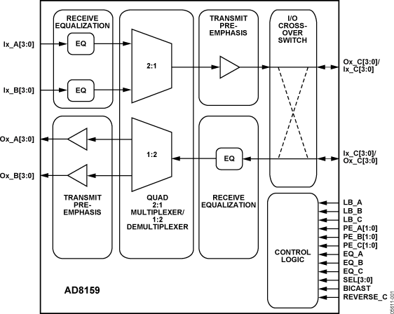
AD8159-EVAL-AC
Analog Devices Inc.The AD8159 is an asynchronous, protocol agnostic, quad-lane 2:1 switch with 12 differential PECL-/CML-compatible inputs and 12 differential CML outputs. The operation of this product is optimized for NRZ signaling with data rates of up to 3.2 Gbps per lane. Each lane offers two levels of input equalization and four levels of output pre-emphasis.The AD8159 consists of four multiplexers and four demultiplexers, one per lane. Each port is a four-lane link, and each lane runs up to a 3.2 Gbps data rate, independent of the other lanes. The lanes are switched independently using the four select pins, SEL[3:0]; each select pin controls one lane of the port. The AD8159 has low latency and very low lane-to-lane skew.The main application of the AD8159 is to support redundancy on both the backplane side and the line interface side of a serial link. The device has unicast and bicast capability; therefore, it can be configured to support either 1 + 1 or 1:1 redundancy.The AD8159 supports reversing of the output and input pins on one of its ports, which helps to connect two ASICs with opposite pinouts.The AD8159 is also used for testing high speed serial links by duplicating incoming data and sending it to the destination port and to the test equipment simultaneously.ApplicationsLow cost redundancy switchSONET OC-48/SDH-16 and lower data ratesXAUI (10 gigabit Ethernet) over backplaneGigabit Ethernet over backplaneFibre Channel 1.06 Gbps and 2.125 Gbps over backplaneInfiniBand? over backplanePCI Express (PCIe) over backplane

AD8189-EVALZ
Analog Devices Inc.The AD8189 (G = 2) is a high speed, single-supply, triple 2-to-1 multiplexer. It offers -3 dB small signal bandwidth of 350 MHz and -3 dB large signal bandwidth of 300 MHz, along with a slew rate in excess of 1000 V/?s. With -84 dB of all hostile crosstalk and -95 dB off isolation, the part is well suited for many high speed applications. The differential gain and differential phase error of 0.05% and 0.05? respectively, along with 0.1 dB flatness to 70 MHz, make the AD8188 ideal for professional and component video multiplexing. The part offers 4 ns switching time, making them an excellent choice for switching video signals, while consuming less than 20 mA on a single 5 V supply (100 mW). The device has a high speed disable feature that sets the outputs into a high impedance state. This allows the building of larger input arrays while minimizing off-channel output loading. The device is offered in a 24-lead TSSOP.

AD8231-EVALZ
Analog Devices Inc.The AD8231 is a low drift, rail-to-rail, instrumentation amplifier with software-programmable gains of 1, 2, 4, 8, 16, 32, 64, or 128. The gains are programmed via digital logic or pin strapping.The AD8231 is ideal for applications that require precision performance over a wide temperature range, such as industrial temperature sensing and data logging. Because the gain setting resistors are internal, maximum gain drift is only 10 ppm/?C for gains of 1 to 32. Because of the auto-zero input stage, maximum input offset is 15 ?V and maximum input offset drift is just 50 nV/?C. CMRR is 80 dB for G = 1, increasing to 110 dB at higher gains.The AD8231 also includes an uncommitted op amp that can be used for additional gain, differential signal driving, or filtering. Like the in-amp, the op amp has an auto-zero architecture, rail-to-rail input, and rail-to-rail output.The AD8231 includes a shutdown feature that reduces current to a maximum of 1 ?A. In shutdown, both amplifiers also have a high output impedance, which allows easy multiplexing of multiple amplifiers without additional switches.The AD8231 is specified over the extended industrial tempera-ture range of ?40?C to +125?C. It is available in a 4 mm ? 4 mm 16-lead LFCSP.Applications Pressure and strain transducers Thermocouples and RTDs Programmable instrumentation Industrial controls Weigh scales Automotive controls

AD8232-EVALZ
Analog Devices Inc.The AD8232 is an integrated signal conditioning block for ECG and other biopotential measurement applications. It is designed to extract, amplify, and filter small biopotential signals in the presence of noisy conditions, such as those created by motion or remote electrode placement. This design allows for an ultralow power analog-to-digital converter (ADC) or an embedded microcontroller to acquire the output signal easily.The AD8232 can implement a two-pole high-pass filter for eliminating motion artifacts and the electrode half-cell potential. This filter is tightly coupled with the instrumentation architec-ture of the amplifier to allow both large gain and high-pass filtering in a single stage, thereby saving space and cost.An uncommitted operational amplifier enables the AD8232 to create a three-pole low-pass filter to remove additional noise. The user can select the frequency cutoff of all filters to suit different types of applications.To improve common-mode rejection of the line frequencies in the system and other undesired interferences, the AD8232 includes an amplifier for driven lead applications, such as right leg drive (RLD).The AD8232 includes a fast restore function that reduces the duration of otherwise long settling tails of the high-pass filters. After an abrupt signal change that rails the amplifier (such as a leads off condition), the AD8232 automatically adjusts to a higher filter cutoff. This feature allows the AD8232 to recover quickly, and therefore, to take valid measurements soon after connecting the electrodes to the subject.The AD8232 is available in a 4 mm ? 4 mm, 20-lead LFCSP and a LFCSP_SS package. Performance for the A grade models is specified from 0?C to 70?C and the models are operational from ?40?C to +85?C. Performance for the W grade models is specified over the automotive temperature range of ?40?C to +105?C.Applications Fitness and activity heart rate monitors Portable ECG Remote health monitors Gaming peripherals Biopotential signal acquisition

AD8273-EVALZ
Analog Devices Inc.The AD8273 is a low distortion, dual-channel amplifier with internal gain setting resistors. With no external components, it can be configured as a high performance difference amplifier (G = ? or 2), inverting amplifier (G = ? or 2), or noninverting amplifier (G = 1? or 3).The AD8273 operates on both single and dual supplies and only requires 2.5 mA maximum supply current for each amplifier. It is specified over the industrial temperature range of ?40?C to +85?C and is fully RoHS compliant.Applications ADC drivers High performance audio Instrumentation amplifier building blocks Level translators Automatic test equipment Sine/cosine encoders

AD8283CP-EBZ
Analog Devices Inc.The AD8283 is designed for low cost, low power, compact size, flexibility, and ease of use. It contains six channels of a low noise preamplifier (LNA) with a programmable gain amplifier (PGA) and an antialiasing filter (AAF) plus one direct-to-ADC channel, all integrated with a single 12-bit analog-to-digital converter (ADC).Each channel features a gain range of 16 dB to 34 dB in 6 dB increments and an ADC with a conversion rate of up to 80 MSPS. The combined input-referred noise voltage of the entire channel is 3.5 nV/?Hz at maximum gain. The channel is optimized for dynamic performance and low power in applications where a small package size is critical.Fabricated in an advanced CMOS process, the AD8283 is available in a 10 mm ? 10 mm, RoHS-compliant, 72-lead LFCSP. It is specified over the automotive temperature range of ?40?C to +105?C.APPLICATIONS Automotive radar Adaptive cruise control Collision avoidance Blind spot detection Self-parking Electronic bumper


