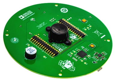
EVAL-ADG5412FEBZ
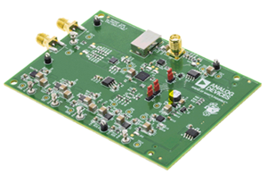
Analog Devices Inc.The ADG5412F and ADG5413F contain four independently controlled single-pole/single-throw (SPST) switches. The ADG5412F has four switches that turn on with Logic 1 inputs. The ADG5413F has two switches with that turn on and two switches that turn off with Logic 1 inputs. Each switch conducts equally well in both directions when on, and each switch has an input signal range that extends to the supplies. The digital inputs are compatible with 3 V logic inputs over the full operating supply range.When no power supplies are present, the switch remains in the off condition, and the switch inputs are high impedance. Under normal operating conditions, if the analog input signal levels on any Sx pin exceed VDD or VSS by a threshold voltage, VT, then the switch turns off. Input signal levels up to +55 V or ?55 V relative to ground are blocked, in both the powered and unpowered condition.The low on resistance of these switches, combined with on-resistance flatness over a significant portion of the signal range make them an ideal solution for data acquisition and gain switching applications where excellent linearity and low distortion are critical.Product Highlights Source pins are protected against voltages greater than the supply rails, up to ?55 V and +55 V. Source pins are protected against voltages between ?55 V and +55 V, in an unpowered state. Overvoltage detection with digital output indicates operating state of switches. Trench isolation guards against latch-up. Optimized for low on resistance and on-resistance flatness. The ADG5412F/ADG5413F can be operated from a dual?supply of ?5 V up to ?22 V or a single power supply of 8 V up to 44 V.Applications Analog input/output modules Process control/distributed control systems Data acquisition Instrumentation Avionics Automatic test equipment Communication systems Relay replacement
EVAL-ADG5436FEBZ
Analog Devices Inc.The ADG5436 is a monolithic CMOS device containing twoindependently selectable single-pole/double-throw (SPDT)switches. An EN input on the LFCSP package enables or disablesthe device. When disabled, all channels switch off. Each switch conducts equally well in both directions when on and has aninput signal range that extends to the supplies. In the off condition,signal levels up to the supplies are blocked. Both switches exhibitbreak-before-make switching action for use in multiplexerapplications.The on-resistance profile is very flat over the full analog input range, ensuring excellent linearity and low distortion when switching audio signals.Product Highlights Trench isolation guards against latch-up. A dielectric trench separates the P and N channel transistors thereby preventing latch-up even under severe overvoltage conditions. Low RON. Dual-supply operation. For applications where the analog signal is bipolar, the ADG5436 can be operated from dual supplies up to ?22 V. Single-supply operation. For applications where the analog signal is unipolar, the ADG5436 can be operated from a single-rail power supply up to 40 V. 3 V logic compatible digital inputs: VINH = 2.0 V, VINL = 0.8 V. No VL logic power supply required.Applications Relay replacement Automatic test equipment Data acquisition Instrumentation Avionics Audio and video switching Communication systems
LT4363IDE-2 Demo Board: 12V System ISO-7637-2 Surge Stopper, Auto-Retry Version
Analog Devices Inc.DC2062A-B: Demo Board for LT4363 High Voltage Surge Stopper with Current Limit.
LTC5577 | 300MHz to 6GHz High Signal Level Active Downconverting Mixer
Analog Devices Inc.Demonstration circuit DC2070A is optimized for evaluation of the LTC5577 high signal level active downconverting mixer. Its RF input port is matched to 50Ω from 1.3GHz to 4.3GHz with 12dB return loss, and the LO port is matched to 50Ω from 950MHz to 4.1GHz with 10dB return loss. The RF and LO inputs are easily matched for higher or lower frequencies with simple external matching, as low as 350MHz and 300MHz, respectively. The low capacitance differential IF output is usable up to 1.5GHz. The LTC5577 active mixer is optimized for RF downconverting applications that require high input signal handling capability and wide bandwidth.
LTC2373-18 Demo Board | 18-Bit, 1Msps, 8-Channel SAR ADC with 100dB SNR (Requires DC590, DC2026 or DC890)
Analog Devices Inc.Demonstration circuit 2071A features the LTC2373 family. The LTC2374/LTC2373/LTC2372 are low noise, high speed, 8-channel, 16/18-bit successive approximation register (SAR) ADCs. The demo manual refers to the LTC2373-18 but applies to all parts in the family, the only differences being the number of bits and the maximum sample rate. Operating from a single 5V supply, the LTC2373-18 has a highly configurable, low crosstalk, 8-channel input multiplexer, supporting fully differential, pseudo-differential unipolar and pseudo-differential bipolar analog input ranges.
LTC2372-16 Demo Board | 16-Bit, 500ksps, 8-Channel SAR ADC with 96dB SNR (Requires DC590, DC2026 or DC890)
Analog Devices Inc.Demonstration circuit 2071A features the LTC2373 family. The LTC2374/LTC2373/LTC2372 are low noise, high speed, 8-channel, 16/18-bit successive approximation register (SAR) ADCs. The demo manual refers to the LTC2373-18 but applies to all parts in the family, the only differences being the number of bits and the maximum sample rate. Operating from a single 5V supply, the LTC2373-18 has a highly configurable, low crosstalk, 8-channel input multiplexer, supporting fully differential, pseudo-differential unipolar and pseudo-differential bipolar analog input ranges.
DC2073B-D
Analog Devices Inc.The LTC6905 precision, programmable silicon oscillator is easy to use and occupies very little board space. It requires only a single resistor to set the output frequency from 17MHz to 170MHz with a typical frequency error of 0.5% or less.The LTC6905 operates with a single 2.7V to 5.5V power supply and provides a rail-to-rail, 50% duty cycle square wave output. The CMOS output driver ensures fast rise/fall times and rail-to-rail switching. Operation is simple: A single resistor, RSET, between 10K to 25K is used to set the frequency, and an internal three-state divider (DIV input) allows for division of the master clock by 1, 2 or 4, providing three frequencies for each RSET value.The LTC6905 features a proprietary feedback loop that linearizes the relationship between RSET and frequency, eliminating the need for tables to calculate frequency. The oscillator can be easily programmed using the simple formula outlined below:See first page of Data Sheet for formula?For higher accuracy, fixed frequency versions that includean internal frequency-setting resistor, see the LTC6905-XXX Series datasheet.Applications High Frequency Precision Oscillator High Speed Data Bus Clock Fixed Crystal Oscillator Replacement Ceramic Oscillator Replacement
DC2073B-G
Analog Devices Inc.The LTC6905-X series of parts are precision, fixed frequency, silicon oscillators designed to minimize board space while maximizing accuracy and ease of use.Programmed at the factory to a fixed frequency, the LTC6905-X series of parts need no external trim components. An internal three-state divider allows for division of the master clock by 1, 2 or 4, providing 3 frequencies (for each device).The LTC6905-X series operate with a single 2.7V to 5.5V power supply and provide a rail-to-rail, 50% duty cycle, square wave output. The OE pin will disable the output when brought low and synchronously enable the output when brought high, avoiding pulse slivers.The four products of the LTC6905-X family are: LTC6905-133: fOSC = 133MHz, 66.7MHz, 33.3MHz LTC6905-100: fOSC = 100MHz, 50MHz, 25MHz LTC6905-96: fOSC = 96MHz, 48MHz, 24MHz LTC6905-80: fOSC = 80MHz, 40MHz, 20MHz?The LTC6905-X series of parts are designed with a factory trim option to modify the divider ratios from 1, 2, 4 to 8, 16, 32. A second trim option allows for additional master clock frequencies. For the alternate divider ratios and unlisted frequencies, contact LTC marketing.Protected by U.S. Patents, including 6614313, 6342817.Applications Data Clocks for High Reliability Applications High Vibration, High Acceleration Environments Replacement for Fixed Crystal and Ceramic Oscillators
DC2073B-H
Analog Devices Inc.The LTC6906 is a precision programmable oscillator that is versatile, compact and easy-to-use. Micropower operation benefits portable and battery-powered equipment. At 100kHz, the LTC6906 consumes 12?A on a 3.3V supply.A single resistor programs the oscillator frequency over a 10:1 range with better than 0.5% initial accuracy. The output frequency can be divided by 1, 3 or 10 to span a 100:1 total frequency range, 10kHz to 1MHz.No decoupling capacitor is needed in most cases, yielding an extremely compact solution occupying less than 20mm2.? Contact LTC Marketing for a version of the part with a shutdown feature or lower frequency operation.The LTC6906 is available in the 6-lead SOT-23 (ThinSOT) package.APPLICATIONS Low Cost Precision Programmable Oscillator Rugged, Compact Micropower Replacement for Crystal and Ceramic Oscillators High Shock and Vibration Environments Portable and Battery-Powered Equipment PDAs and Cellular Phones
LTM4630EV Demo Board | Step-Down μModule Regulator, 4.5V ≤ VIN ≤ 15V, VOUT = 1V @ 36A
Analog Devices Inc.Demonstration circuit 2081A-A features the LTM4630EV, the high efficiency, high density, dual 18A, switch mode step-down μModule® regulator. The input voltage is from 4.5V to 15V. The output voltage is programmable from 0.6V to 1.8V. DC2081A-A is configured as dual-phase, single-output, which can deliver up to 36A maximum. The board designs with minimum components to demonstrate this high efficiency, high density μModule. As explained in the data sheet, output current de-rating is necessary for certain VIN, VOUT, and thermal conditions.
LTC2000A-11 Demo Board | 11-Bit, 2.7Gsps DAC with DDR LVDS Interface
Analog Devices Inc.Demonstration circuit 2085 supports the LTC2000 and LTC2000A, a high speed, high dynamic range family of DACs. It was specially designed for applications that require differential DC coupled outputs. DC2085 supports the complete family of the LTC2000 including 16, 14 and 11 bit parts.
Companion Board : Stratix board
LTC1559CS8-5 | Single Cell Backup Supply, 5V @ 3A VOUT (Normal) and 5V @ 20mA VOUT (Backup)
Analog Devices Inc.DC208A-B: Demo Board for the LTC1559 Backup Battery Controller with Fixed Output.
LTC5599 | 30MHz to 1300MHz Low Power Direct I/Q Modulator - DC590B Serial Board Required
Analog Devices Inc.Demonstration circuit 2091A is optimized for evaluation of the LTC5599 low power direct quadrature modulator. The balanced I and Q baseband input ports can be either AC- or DC-coupled to a source with a common mode voltage level of about 1.4V. Fixed LC networks on the LO and RF ports cover a continuous 90MHz to 1300MHz range. The SPI interface controls the supply current, modulator gain, and allows optimization of the LO carrier feedthrough and side-band suppression.
LT4275A/LT4321 LTPoE++/PoE+/PoE PD Demo Board
Analog Devices Inc.DC2093A-A Demo Board for:
LT4275 LTPoE++/PoE+/PoE PD Controller
LT4321 PoE Ideal Diode Bridge Controller
LTC3630AEMSE Demo Board (MSOP) | 4V ≤ VIN ≤ 76V, VOUT = 1.8V/3.3V/5V/Adjustable @ 500mA
Analog Devices Inc.Demonstration circuit 2105A is a 500mA output DC/DC power supply. There are two versions: DC2105A-A is a board featuring LTC3630A in the exposed pad MSOP-16 package, with 4V to 76V input range; DC2105A-B is a board featuring LTC3630, with 4V to 65V input range. The LTC3630A operates in a high efficiency Burst Mode® operation and includes internal high and low side switches. The board provides jumper selected output voltages of 1.8V, 3.3V, 5V and an option for additional voltages. LTC3630A has internal soft-start and a provision for increasing soft-start time.
LTC3630EMSE Demo Board | 4V ≤ VIN ≤ 65V, VOUT = 1.8V/3.3V/5V/Adjustable @ 500mA
Analog Devices Inc.Demonstration circuit 2105A is a 500mA output DC/DC power supply. There are two versions: DC2105A-A is a board featuring LTC3630A, with 4V to 76V input range; DC2105A-B is a board featuring LTC3630, with 4V to 65V input range. The LTC3630 operates in a high efficiency Burst Mode® operation and includes internal high and low side switches. The board provides jumper selected output voltages of 1.8V, 3.3V, 5V and an option for additional voltages. LTC3630 has internal soft-start and a provision for increasing soft-start time.
DC2110A
Analog Devices Inc.The LT8631 is a current mode PWM step-down DC/DC converter with internal synchronous switches that provide current for output loads up to 1A. The wide input range of 3V to 100V makes the LT8631 suitable for regulating power from a wide variety of sources, including automotive and industrial systems and 36V to 72V telecom supplies. Low ripple Burst Mode operation enables high efficiency operation down to very low output currents while keeping the output ripple below 10mVP-P. Resistor programmable 100kHz to 1MHz frequency range and synchronization capability enable optimization between efficiency and external component size. The soft-start feature controls the ramp rate of the output voltage, eliminating input current surge during start-up, while also providing output tracking. A power good flag signals when the output voltage is within ?7.5% of the regulated output. Undervoltage lockout can be programmed using the EN/UV pin. Shutdown mode reduces the total quiescent current to < 5?A. The LT8631 is available in a 20-lead TSSOP package with exposed pad for low thermal resistance and high voltage lead spacing.APPLICATIONS Automotive Supplies Telecom Supplies Distributed Supply Regulation
DC2113A
Analog Devices Inc.The LTC3649 is a high efficiency 60V, 4A synchronous monolithic step-down regulator. The regulator features a single resistor programmable output voltage, internal compensation and high efficiencies over a wide VOUT range.The step-down regulator operates from an input voltage range of 3.1V to 60V and provides an adjustable rail-to-rail output range from (VIN ? 0.5V) to ground while delivering up to 4A of output current. The switching frequency is also adjusted with an external resistor. A user-selectable mode input is provided to allow the user to trade off ripple noise for efficiency at light loads; Burst Mode operation provides the highest efficiency at light loads, while forced continuous mode provides low output ripple. The MODE/SYNC pin can also be used to allow the user to synchronize the switching frequency to an external clock.The LTC3649 operates with a peak current mode architecture that allows for fast transient response with inherent cycle-to-cycle current limit protection. It also features programmable output current limit, current monitoring and input voltage regulation.Applications Industrial Applications Automotive Applications
LTC4234 Demo Board | 20A Guaranteed SOA Hot Swap Controller
Analog Devices Inc.Demonstration circuit 2116A features the LTC4233/LTC4234 10A/20A Guaranteed SOA Hot Swap™ Controllers. The LTC4233 and LTC4234 are ideally suited for compact power distribution control in 2.9V to 15V applications for hot board insertion protection, high side power switching, and electronic circuit breaker functions.
LTC3895EFE Demo Board | Synchronous Buck, 14V ≤ VIN ≤ 130V, 150VPK; VOUT = 12V @ 5A
Analog Devices Inc.Demonstration circuit 2117A is a single output high voltage nonisolated synchronous step-down converter that drives all N-channel MOSFET power stage. It features the LTC3895EFE, a high voltage step-down DC/DC controller housed in a TSSOP-38 package with several pins removed for high voltage spacing.


