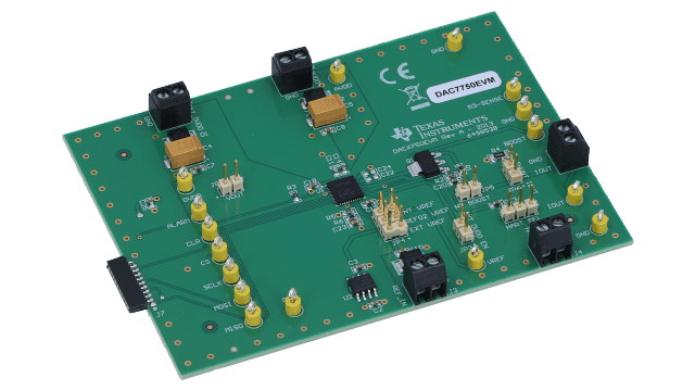
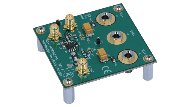
DAC7750 12-Bit Programmable DAC With 4mA-to-20mA Current Output Evaluation Module
Texas InstrumentsDAC7750 12-Bit Programmable DAC With 4mA-to-20mA Current Output Evaluation Module


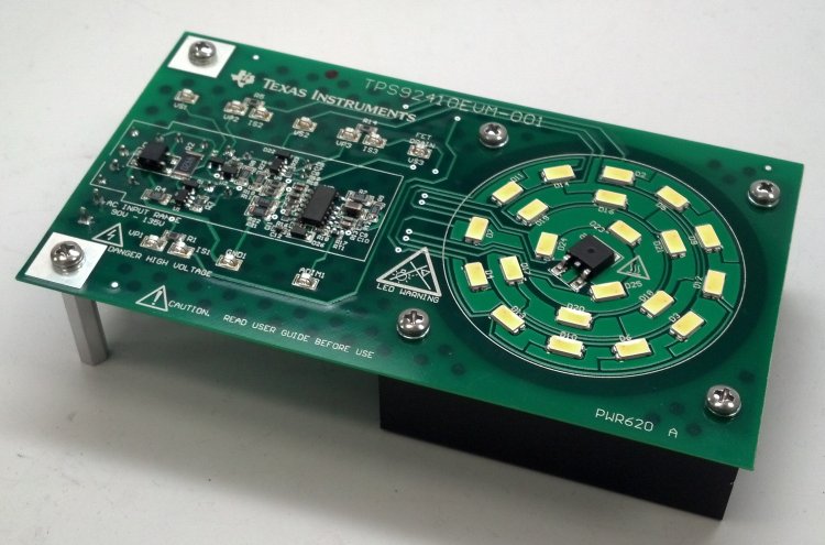
LM3414 LM3414HV 1A 65V LED Driver PSOP-8 Evaluation Board
Texas InstrumentsLM3414 LM3414HV 1A 65V LED Driver PSOP-8 Evaluation Board

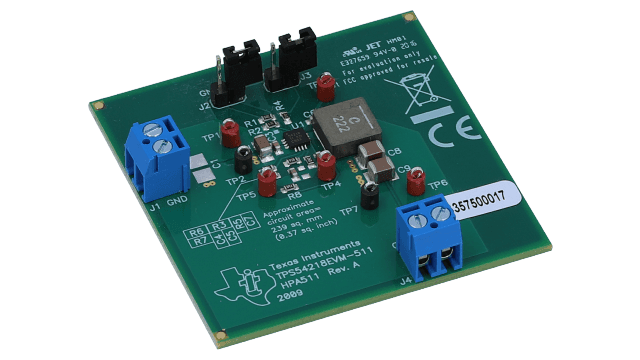
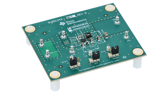
TPS54218 6V Input; 1.8V Output; 2A SWIFT™ Converter Evaluation Module
Texas InstrumentsTPS54218 6V Input; 1.8V Output; 2A SWIFT™ Converter Evaluation Module

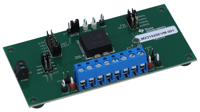
LMZ31520 3V to 14.5V; 20A Step-Down Power Module Evaluation Board
Texas InstrumentsLMZ31520 3V to 14.5V; 20A Step-Down Power Module Evaluation Board
Evaluation Board for the LM3433 10A to 40A LED Driver
Texas InstrumentsEvaluation Board for the LM3433 10A to 40A LED Driver
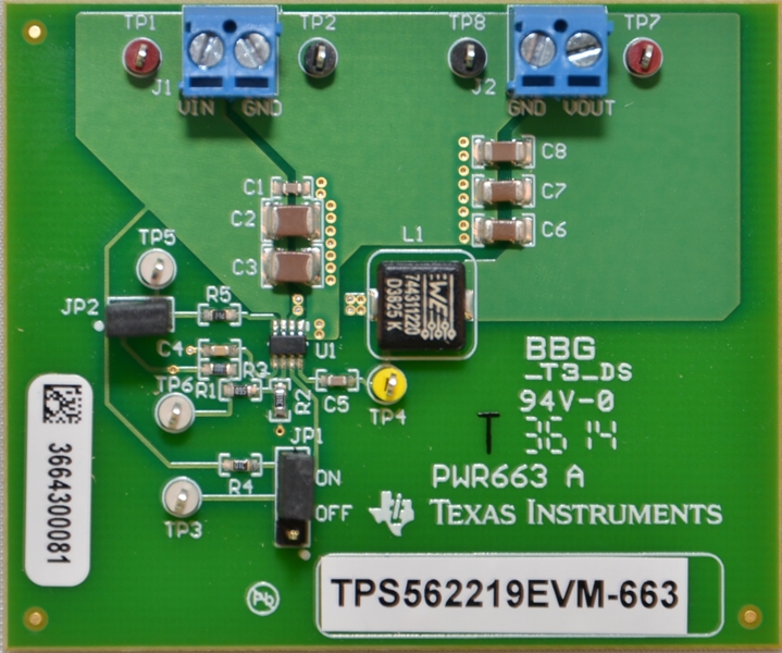
TPS562219 17V Input, 2A Synchronous Step-Down Regulator in SOT-23 Evaluation Module
Texas InstrumentsTPS562219 17V Input, 2A Synchronous Step-Down Regulator in SOT-23 Evaluation Module
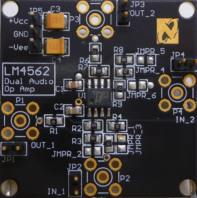
Dual High Performance; High Fidelity Audio Operational Amplifier (8-pin; SOIC Narrow)
Texas InstrumentsDual High Performance; High Fidelity Audio Operational Amplifier (8-pin; SOIC Narrow)
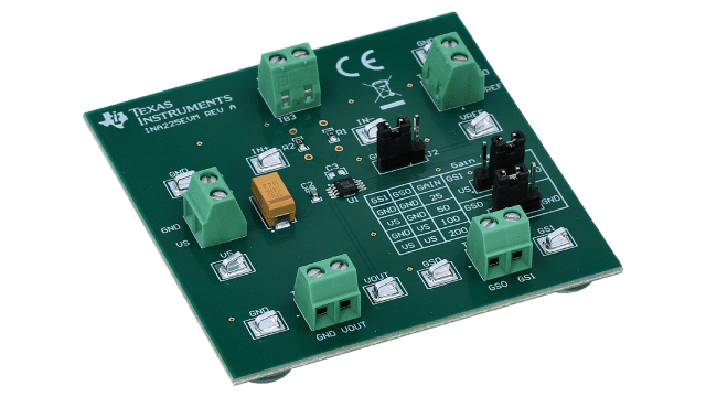
INA225 Evaluation Module for 36-V Programmable-Gain; Current Shunt Monitor
Texas InstrumentsINA225 Evaluation Module for 36-V Programmable-Gain; Current Shunt Monitor
THS3091 evaluation module for single; high-voltage low-distortion current-feedback op amp
Texas InstrumentsTHS3091 evaluation module for single; high-voltage low-distortion current-feedback op amp

700nA Low Iq Highly Integrated Battery Chg Management Solution for Wearables & IoT Evaluation Module
Texas Instruments700nA Low Iq Highly Integrated Battery Chg Management Solution for Wearables & IoT Evaluation Module
TPS2330 48-V Telecom Hot Swap Evaluation Module and Interface Card
Texas InstrumentsTPS2330 48-V Telecom Hot Swap Evaluation Module and Interface Card
LM53600-Q1 Adjustable Output; 650mA Buck Regulator Evaluation Module With Spread Spectrum
Texas InstrumentsLM53600-Q1 Adjustable Output; 650mA Buck Regulator Evaluation Module With Spread Spectrum


