
LT6658-1.2 Demo Board | Low Noise, High Current, Precision Reference
Analog Devices Inc.Demonstration circuit 2432B features the LT6658, a precision dual output reference that combines the performance of a low drift low noise reference and a linear regulator. Demonstration circuits are available with 1.25V, 1.8V, 2.5V, 3.0V, 3.3V and 5V output option parts. Both outputs are ideal for driving the precision reference inputs of high resolution ADCs and DACs, even with heavy loading while simultaneously acting as output supplies for powering microcontrollers and other supporting devices. Both outputs have the same precision specifications and A track each other over temperature. Each output can be configured with external resistors to give an output voltage up to 6V.
LT6658-3.3 Demo Board | Low Noise, High Current, Precision Reference
Analog Devices Inc.Demonstration circuit 2432B features the LT6658, a precision dual output reference that combines the performance of a low drift low noise reference and a linear regulator. Demonstration circuits are available with 1.25V, 1.8V, 2.5V, 3.0V, 3.3V and 5V output option parts. Both outputs are ideal for driving the precision reference inputs of high resolution ADCs and DACs, even with heavy loading while simultaneously acting as output supplies for powering microcontrollers and other supporting devices. Both outputs have the same precision specifications and A track each other over temperature. Each output can be configured with external resistors to give an output voltage up to 6V.
LT6658-5 Demo Board | Low Noise, High Current, Precision Reference
Analog Devices Inc.Demonstration circuit 2432B features the LT6658, a precision dual output reference that combines the performance of a low drift low noise reference and a linear regulator. Demonstration circuits are available with 1.25V, 1.8V, 2.5V, 3.0V, 3.3V and 5V output option parts. Both outputs are ideal for driving the precision reference inputs of high resolution ADCs and DACs, even with heavy loading while simultaneously acting as output supplies for powering microcontrollers and other supporting devices. Both outputs have the same precision specifications and A track each other over temperature. Each output can be configured with external resistors to give an output voltage up to 6V.

DC2438A
Analog Devices Inc.The LTM2894 is a complete galvanically-isolated USB 2.0 compatible ?Module? (micromodule) transceiver.The LTM2894 is ideal for isolation in host, hub, bus splitter or peripheral device applications. It is compatible with USB 2.0 full speed (12Mbps) and low speed (1.5Mbps) operation. Automatic speed selection configures integrated pull-up resistors on the upstream port to match those sensed on the downstream device.The isolator ?Module technology uses coupled inductors to provide 7500VRMS of isolation and 17.4mm of creepage between the upstream and downstream USB interface. This device is ideal for systems requiring isolated ground returns or large common mode voltage variations. Uninterrupted communication is guaranteed for common mode transients greater than 50kV/?s.Enhanced ESD protection allows this part to withstand up to ?20kV (human body model) on the USB transceiver interface pins to local supplies and ?20kV through the isolation barrier to supplies without latch-up or damage.Applications Isolated USB Interfaces Host, Hub, or Device Isolation Industrial/Medical Data Acquisition

LTM4636 High Efficiency, PolyPhase 160A Step-Down Power µModule Regulator
Analog Devices Inc.Demonstration circuit DC2448A-C features a PolyPhase® design using the LTM4636EY, a 40A high efficiency, switch mode step-down power µModule® regulator. The input voltage range is from 4.7V to 15V. When VIN < 5.5V, short PVCC to VIN with R1 = 0Ω, and set R3 = 0Ω and remove R2. The output voltage range is 0.6V to 3.3V. The DC2448A-C can deliver a nominal 160A output current. As explained in the data sheet, output current derating is necessary for certain VIN, VOUT and thermal conditions. The board operates in continuous conduction mode in heavy load conditions. For high efficiency at low load currents, the MODE_PLLIN jumper selects pulse-skipping mode for noise sensitive applications or Burst Mode® operation in less noise sensitive applications. The MODE_PLLIN pin also allows the LTM4636 to synchronize to an external clock signal. The phases of the four LTM4636s are 0 degree, 90 degree, 180 degree and 270 degree. DC2448A-C has the option of choosing both internal and external compensation circuit for LTM4636. The LTM4636 datasheet must be read in conjunction with this demo manual prior to working on or modifying demo circuit DC2448A-C.

LTM4643 Demo Board | Quad Buck μModule Regulator with Configurable 3A Output Array
Analog Devices Inc.Demonstration circuit 2453A features the LTM4643 μModule® regulator, a high performance high efficiency 4 output step-down regulator. The LTM4643EV has an operating input voltage range of 4V to 14V and is able to provide up to 3A out output current from each of its phases. Each output’s voltage is programmable from 0.6V to 5.5V but the demo board is configured to provide outputs of 3.3V, 2.5V, 1.5V and 1.2V. The LTM4643EV is a complete DC/DC point of load regulator in a thermally enhanced 15mm × 9mm × 5.01mm BGA package requiring only a few input and output capacitors.

DC2468A
Analog Devices Inc.The LT8645S/LT8646S synchronous step-down regulator features second generation Silent Switcher architecture designed to minimize EMI emissions while delivering high efficiency at high switching frequencies. This includes the integration of bypass capacitors to optimize all the fast current loops inside and make it easy to achieve advertised EMI performance by eliminating layout sensitivity.The fast, clean, low-overshoot switching edges enable high efficiency operation even at high switching frequencies, leading to a small overall solution size. Peak current mode control with a 40ns minimum on-time allows high step-down ratios even at high switching frequencies. The LT8646S has external compensation to enable current sharing and fast transient response at high switching frequencies.Burst Mode? operation enables ultralow standby current consumption, pulse-skipping mode allows full switching frequency at lower output loads, or spread spectrum operation can further reduce EMI emissions.Applications Automotive and Industrial Supplies General Purpose Step-Down GSM Power Supplies

DC2479A-B
Analog Devices Inc.The LTM4650-1A/LTM4650-1B is dual 25A or single 50A output step-down ?Module? (power module) regulator with ?0.8% (LTM4650-1A) and ?1.5% (LTM4650-1B) total DC output error with ?3% transient output error. Included in the package are the switching controller, power FETs, inductors, and all supporting components. External compensation allows for fast transient response to minimize output capacitance when powering FPGAs, ASICs, and processors. With synchronized multiphase parallel current sharing, six LTM4650-1 devices can deliver up to 300A. The LTM4650-1 is offered in a 16mm ? 16mm ? 5.01 BGA package, with SnPb (BGA) or RoHS compliant terminal finish. VIN Range VOUT Range Comp DC VOUT Accy LTM4650 4.5V to 15V 0.6V to 1.8V Internal 1.5% LTM4650-1B 4.5V to 15V 0.6V to 1.8V External 1.5% LTM4650-1A 4.5V to 15V 0.6V to 1.8V External 0.8% LTM4650A 4.5V to 16V 0.6V to 5.5V Internal 1% LTM4650A-1 4.5V to 16V 0.6V to 5.5V External 1% Applications FPGA, ASIC, ?Processor Core Voltage Regulation Information, Communication Systems

DC2487A
Analog Devices Inc.The LTC6363 family consists of four fully differential, low power, low noise amplifiers with rail-to-rail outputs optimized to drive SAR ADCs. The LTC6363 is a standalone differential amplifier, where the gain is typically set using four external resistors. The LTC6363-0.5, LTC6363-1, and LTC6363-2 each have internal matched resistors to create fixed gain blocks with gains of 0.5V/V, 1V/V, and 2V/V respectively. Each of the fixed-gain amplifiers features precision laser trimmed on-chip resistors for accurate, ultrastable gain and excellent CMRR.Applications 20-Bit, 18-Bit and 16-Bit SAR ADC Drivers Single-Ended-to-Differential Conversion Low Power ADC Drivers Level Shifter Differential Line Drivers Battery-Powered Instrumentation

DC2494A
Analog Devices Inc.The LTM8063 is a 40VIN, 2A continuous, 2.5A peak, step-down ?Module? (power module) regulator. Included in the package are the switching controller, power switches, inductor, and all support components. Operating over an input voltage range of 3.2V to 40V, the LTM8063 supports an output voltage range of 0.8V to 15V and a switching frequency range of 200kHz to 2.2MHz, each set by a single resistor. Only the input and output filter capacitors are needed to finish the design.The low profile package enables utilization of unused space on the bottom of PC boards for high density point of load regulation. The LTM8063 is packaged in a thermally enhanced, compact over-molded ball grid array (BGA) package suitable for automated assembly by standard surface mount equipment. The LTM8063 is RoHS compliant.Applications Automotive Battery Regulation Power for Portable Products Distributed Supply Regulation Industrial Supplies Wall Transformer Regulation

DC2496A-KIT
Analog Devices Inc.The LTC6432-15 is an ultra-high dynamic range differentialgain block amplifier designed to drive high resolution,high speed ADCs. It offers a full GHz of data bandwidt h forcomplex spectrally efficient modulations schemes or wh ereresistance to blockers is critical. This unique device cansimultaneously achieve low noise, incomparable linearity and flat gain over the 100kHz to 1GHz band.Unlike wideband GaAs PHEMTs, MESFETs and GaN FETs, this SiGe based amplifier exhibits low 1/f noise and can be used down to 100kHz.The LTC6432-15 is designed for ease of use requiring a minimum of support components. Impedance matching, temperature compensation and bias control are handled internally to ensure consistent performance over environmental changes.All A-Grade LTC6432-15 devices are tested and guaranteed for OIP3 at 150MHz. The LTC6432-15 is housed in a 4mm ? 4mm, 24L, QFN package with an exposed pad for thermal management and low inductance. For a single-ended 50? IF Gain Block with similar performance, see the related LTC6433-15.Applications Differential 1GHz Bandwidth ADC Driver Wideband Test Instrument Amplifier Differential IF Amplifier 50?/75? Balanced IF Amplifier

LTC1682CMS8 | Doubler Charge Pump with Linear Regulator, Adjustable, 1.8 to 4.4VIN, 2.5 to 5.5VOUT @ 50mA
Analog Devices Inc.DC249A-A: Demo Board for the LTC1682 Doubler Charge Pumps with Low Noise Linear Regulator.
LTC1682CMS8-5 | Doubler Charge Pump with Linear Regulator, Fixed, 2.7 to 4.4VIN, 5.0VOUT @ 50mA
Analog Devices Inc.DC249A-B: Demo Board for the LTC1682 Doubler Charge Pumps with Low Noise Linear Regulator.

LTM8002 40VIN, 2.5A Step-Down µModule Regulator
Analog Devices Inc.Demonstration circuit 2501A features the LTM®8002, a 40V, 2.5A step-down µModule® regulator. This demo circuit is configured to deliver a 5.0V output from an input
voltage between 6.0V to 40V at a switching frequency of 1MHz. The wide input range of the LTM8002 allows a variety of input sources such as automotive batteries and industrial supplies. Under light load conditions, the available Burst Mode® operation supports high efficiency with low output ripple.
The demo board has an EMI filter installed. The EMI performance of the board is shown in Figure 6 and Figure 7.
The LTM8002 data sheet gives complete description of the device, operation and application information. The data sheet must be read in conjunction with this demo manual prior to working on or modifying demo circuit 2501A.

DC2504A
Analog Devices Inc.The LT8630 is a current mode PWM step-down DC/DC converter with internal synchronous switches that provide current for output loads up to 0.6A. The wide input range of 3V to 100V makes the LT8630 suitable for regulating power from a wide variety of sources, including automotive and industrial systems and 36V to 72V telecom supplies. Variable frequency boundary mode switching maximizes efficiency across a wide range of input voltages. Low ripple Burst Mode operation enables high efficiency operation down to very low output currents while keeping the output ripple below 5mV. The soft-start feature controls the ramp rate of the output voltage, eliminating input current surge during start-up, while also providing output tracking. A power good flag signals when the output voltage is within ?7.5% of the regulated output. Undervoltage lockout can be programmed using the EN/UV pin. Shutdown mode reduces the total quiescent current to < 5?A. The LT8630 is available in a 20-lead TSSOP package with exposed pad for low thermal resistance and high voltage lead spacing.APPLICATIONS Automotive Supplies Telecom Supplies Distributed Supply Regulation

LTC1503CMS8-2 | High Efficiency Inductorless Step-Down DC/DC Converter, 2.4 to 6VIN, 2VOUT @ 100mA
Analog Devices Inc.DC250A-A: Demo Board for the LTC1503 High Efficiency Inductorless Step-Down DC/DC Converter.

LTC2975 Demo Board: ±12V, ±48V Power Supply Management [requires DC1613]
Analog Devices Inc.The DC2518A is a demonstration system for the LTC2975 Power System Manager that interfaces to various regulators. The board contains all the circuitry needed to use the LTC2975 in a power system and control four power supplies. The four power supplies include linear and switching regulators for the purpose of demonstrating a variety of methods to sense voltage and current. The demo board provides a sophisticated, digitally programmable 4-channel power supply system.

DC2527A-B
Analog Devices Inc.The LTM4646 is a complete dual 10A output switching mode DC/DC power supply. Included in the package are the switching controller, power FETs, inductors, and all supporting components. Operating from an input voltage range of 4.5V to 20V, the LTM4646 supports two outputs each with an output voltage range of 0.6V to 5.5V, set by external resistors. Its high efficiency design delivers up to 10A continuous current for each output. Only a few input and output capacitors are needed.The device supports frequency synchronization, multiphase operation, high efficiency light load operation and output voltage tracking for supply rail sequencing and has an on-board temperature diode per channel for device temperature monitoring. High switching frequency and a current mode architecture enable a very fast transient response to line and load changes without sacrificing stability.Fault protection features include overvoltage and overcurrent protection. The power module is offered in a small footprint 11.25mm ? 15mm ? 5.01mm BGA package. The LTM4646 is available with SnPb or RoHS compliant terminal finish.Applications Point-of-Load Power Supplies Telecom and Networking Equipment Industrial Equipment Medical Equipment

LTC7810ELXE High Input Voltage Dual Output Synchronous Buck Converter
Analog Devices Inc.Demonstration circuit 2529A is a dual output synchronous buck converter featuring the LTC7810ELXE in a 48-lead eLQFP package.
Key features of this board include: an optional on-board NMOS LDO for DRVCC; jumper for spread-spectrum option; optional resistors for single output dual phase operation; a mode selector that allows the converter to run in CCM, pulse-skipping, adjustable burst clamp or default Burst Mode® operation; SYNC turret for Poly-Phase® operation.
The input voltage range of this demo board is from 16V to 130V and it uses a sense resistor for overcurrent protection. The LTC7810 data sheet gives a complete description of the part, operation and application information and must be read in conjunction with this demo manual for DC2529A.
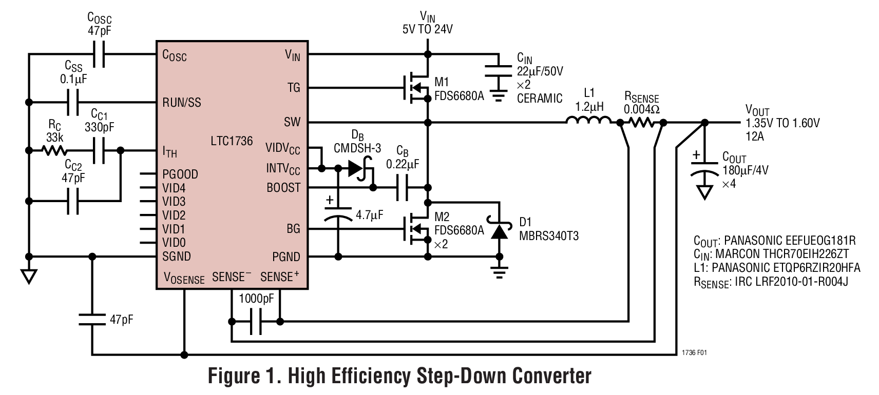
LTC1736CG | 5 Bit, VID CPU Power Converter, VIN = 5V to 24V, VOUT = 0.9V to 2.0V @ 12A
Analog Devices Inc.DC252A: Demo Board for the LTC1736 5-Bit Adjustable High Efficiency Synchronous Step-Down Switching Regulator.


