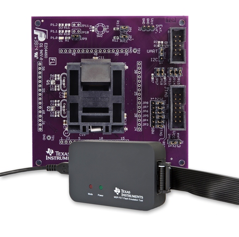
MSP-FET430U64F - MSP430 64-pin FRAM TS Board and MSP-FET Bundle (Microcontrollers not included)
Texas InstrumentsMSP-FET430U64F - MSP430 64-pin FRAM TS Board and MSP-FET Bundle (Microcontrollers not included)
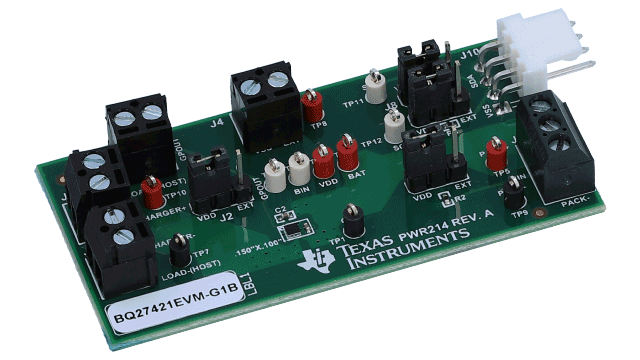
BQ27421EVM-G1B System-Side Battery Fuel (Gas) Gauge Evaluation Module
Texas InstrumentsBQ27421EVM-G1B System-Side Battery Fuel (Gas) Gauge Evaluation Module
LM3668Q1 Synchoronous buck-boost DC/DC converter EVM for automotive application
Texas InstrumentsLM3668Q1 Synchoronous buck-boost DC/DC converter EVM for automotive application
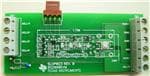
bq2060AEVM-002 Evaluation Kit for NiMH Cells
Texas Instrumentsbq2060AEVM-002 Evaluation Kit for NiMH Cells
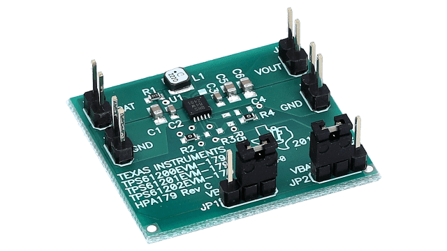
Evaluation Module for TPS79501 Single Output LDO
Texas InstrumentsEvaluation Module for TPS79501 Single Output LDO
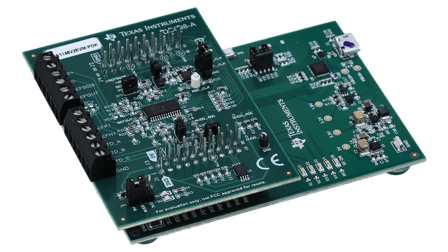
ADS1148 performance demonstration kit for 16-bit 2-kSPS ADC with PGA for sensor measurement
Texas InstrumentsADS1148 performance demonstration kit for 16-bit 2-kSPS ADC with PGA for sensor measurement
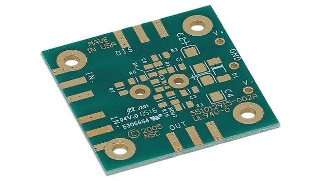
Evaluation Board for High-Speed Single Op Amp in the 5- 6-Pin SC-70 Package
Texas InstrumentsEvaluation Board for High-Speed Single Op Amp in the 5- 6-Pin SC-70 Package
Series 2000 Low Frequency Micro RFID Evaluation Kit
Texas InstrumentsSeries 2000 Low Frequency Micro RFID Evaluation Kit
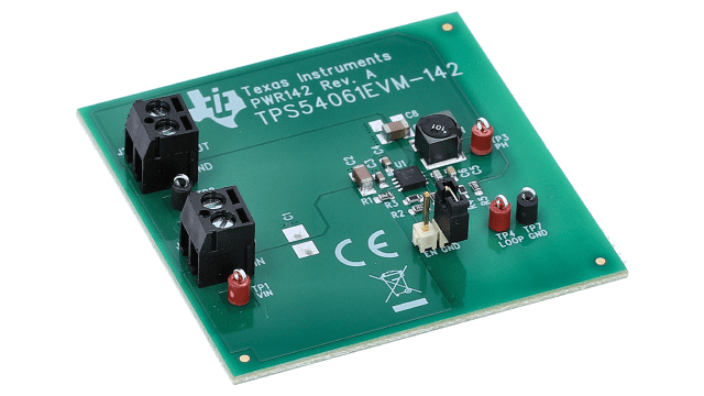
80V Wide Vin Step Down Switching Regulator Evaluation Board
Texas Instruments80V Wide Vin Step Down Switching Regulator Evaluation Board
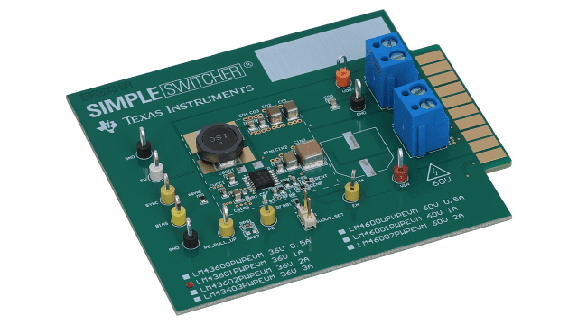
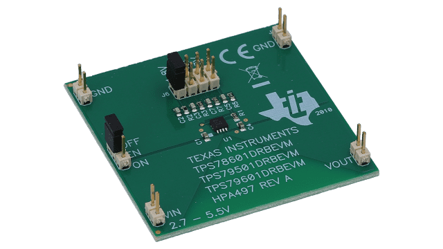
LM43601PWP Synchronous Step-Down Converter Evaluation Module
Texas InstrumentsLM43601PWP Synchronous Step-Down Converter Evaluation Module


