LM34917AEVAL 33V, 1.3A Step-Down Switching Regulator with Over-Voltage Shutdown EVM
Texas InstrumentsLM34917AEVAL 33V, 1.3A Step-Down Switching Regulator with Over-Voltage Shutdown EVM
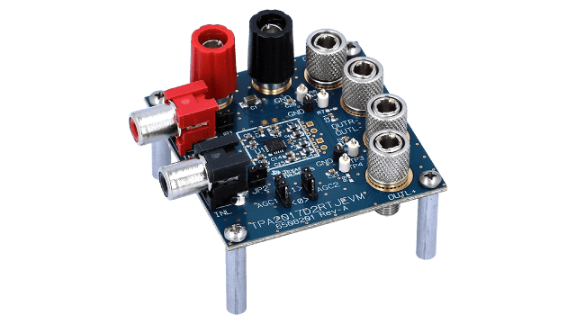
3 Gbps HD SD SDI Configurable I O Adaptive Cable Equalizer Cable Driver Evaluation Board
Texas Instruments3 Gbps HD SD SDI Configurable I O Adaptive Cable Equalizer Cable Driver Evaluation Board
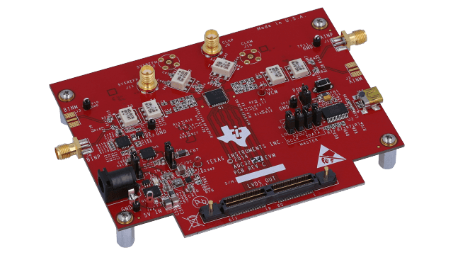
ADC3224 Dual-Channel; 12-Bit; 125-MSPS Analog-to-Digital Converter Evaluation Module
Texas InstrumentsADC3224 Dual-Channel; 12-Bit; 125-MSPS Analog-to-Digital Converter Evaluation Module
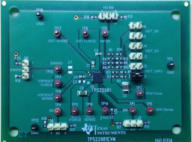
TPS22981 Thunderbolt Host/Peripheral Power MUX Evaluation Module
Texas InstrumentsTPS22981 Thunderbolt Host/Peripheral Power MUX Evaluation Module
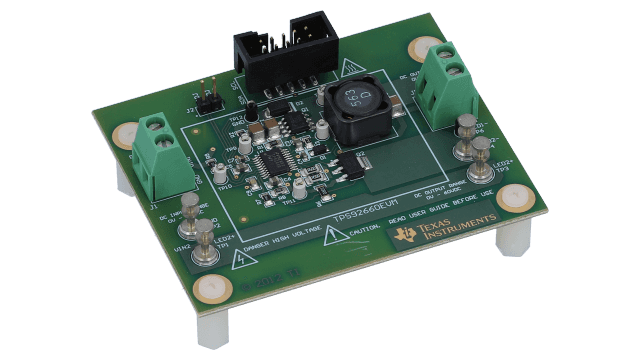
Two String LED Driver with I2C/EPROM Current Trim Evaluation Module Board
Texas InstrumentsTwo String LED Driver with I2C/EPROM Current Trim Evaluation Module Board
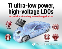
Automotive LDO for Car Battery Direct Connection
Texas InstrumentsBroadening the largest portfolio of low drop-out regulators (LDOs), TI introduces a new family of AEC-Q100-qualified high-voltage LDOs for automotive and industrial applications. With ultra-low quiescent current and the ability to support an input voltage up to 60-V, the LDOs support many applications that connect directly to a car or truck battery, such as cluster, door modules, power steering, infotainment systems and lighting controls.
Key features and benefits of the LDO family for direct connection to the car battery:
Ultra-low quiescent current as low as 10 uA: Lowest quiescent current in standby mode means lower power consumption and increased battery endurance time.
Internal ESR compensation offers the flexibility to use a wide range of output capacitors, including ceramic: Flexibility allows the customer to choose from a wide range of output ceramic capacitors to reduce system cost and increase stability.
High-input voltage allows designers to connect direct to the car battery: Up to 40-V Vin for normal operation and 45-V transient (TPS7A16xx-Q1 can support up to 60-V normal operation for trucks and heavy-duty equipment)
Tracking function provides close to zero tolerance between on-board and off-board power supplies: Tracking helps customers get more accurate data from the off-board sensors..
Integrated window watchdog: enables higher functional safety to be designed into end equipments.
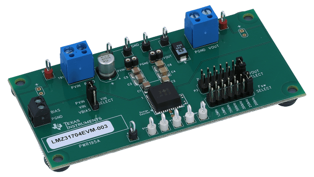
LMZ31704 2.95V to 17V; 4A Step-Down Power Module Evaluation Board
Texas InstrumentsLMZ31704 2.95V to 17V; 4A Step-Down Power Module Evaluation Board
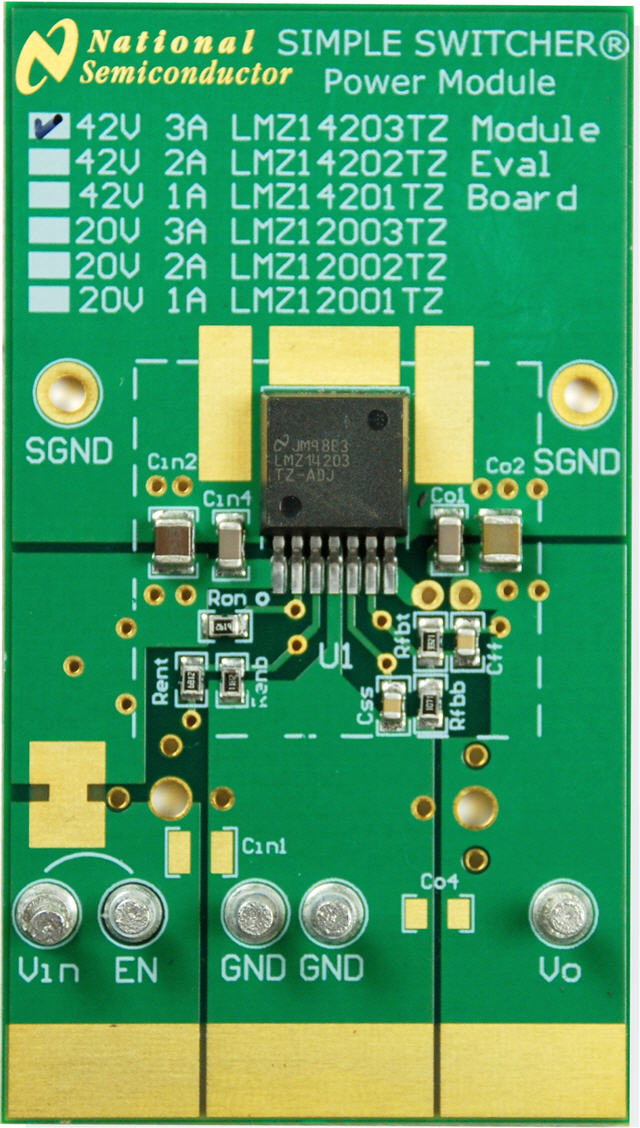
Simple Switcher ® Power Module 42Vin; 1A Eval Board
Texas InstrumentsSimple Switcher ® Power Module 42Vin; 1A Eval Board
Target Development Board (MSP-TS430RGE24A) and MSP-FET Bundle (Microcontrollers Not Included)
Texas InstrumentsTarget Development Board (MSP-TS430RGE24A) and MSP-FET Bundle (Microcontrollers Not Included)
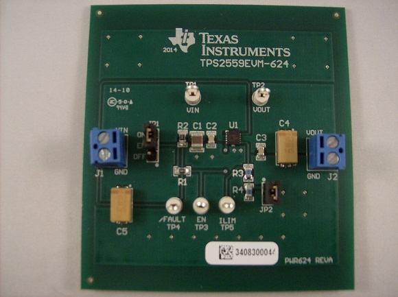
TPS2559EVM-624 Precision Adjustable Current-Limited Power Distribution Switch
Texas InstrumentsTPS2559EVM-624 Precision Adjustable Current-Limited Power Distribution Switch


