
DAC Sample and Hold Glitch Reduction Reference Design
Description
DAC R-2R architectures display great performance in regards to noise and accuracy: but at a cost of large glitch area. This design focuses on the reduction of major-carry glitches that occur from code specific transitions in DAC R-2R architectures. This design reduces this glitch area: making it suitable for glitch-sensitive applications such as waveform generation.
Features
- 18-bit: 0-5 V output R-2R DAC with S&H Glitch Reduction Circuitry
Applications
- Oscilloscopes & digitizers
- Battery cell formation & test equipment
- Vector signal transceiver (VST)
- Wireless communications test
Product Categories
- Data converters
| Download |
|---|
| Download the bill of materials for TIPD142 | Download |

Design File
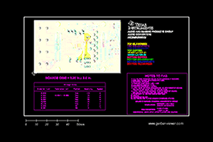
Download ready-to-use system files to speed your design process. Get Viewer.
Download the design file for TIPD142Test Data

Get results faster with test and simulation data that's been verified.
Download the test file for TIPD142| Title | Updated | Type | Size (KB) | |
|---|---|---|---|---|
| TIPD142 BOM | 09 Sep 2015 | 23 | ||
| TIPD142 Schematic | 09 Sep 2015 | 57 |