Search results
LTC3704EMS Demo Board | 4.5V to 15VIN, –70VOUT1 @ 200mA, –24VOUT2 @ 200mA

Analog Devices Inc.
LTC3704EMS Demo Board | 4.5V to 15VIN, –70VOUT1 @ 200mA, –24VOUT2 @ 200mA
Analog Devices Inc.
Demonstration circuit 518 is a SLIC (Subscriber Line Interface Circuit) positive input to negative output converter featuring the LTC3704 switching controller. DC518 converts 4.5V to 15V input to –24V at 200mA and –70V at 200mA at its output. The demo board uses a transformer with the three primary side widings in parallel to generate three –24V outputs. By stacking the voltages on top of each other, –70V ±10% is obtained. The demo board operates at 200kHz with high efficiency of up to 92%.

DC2141A
Analog Devices Inc.
DC2141A
Analog Devices Inc.
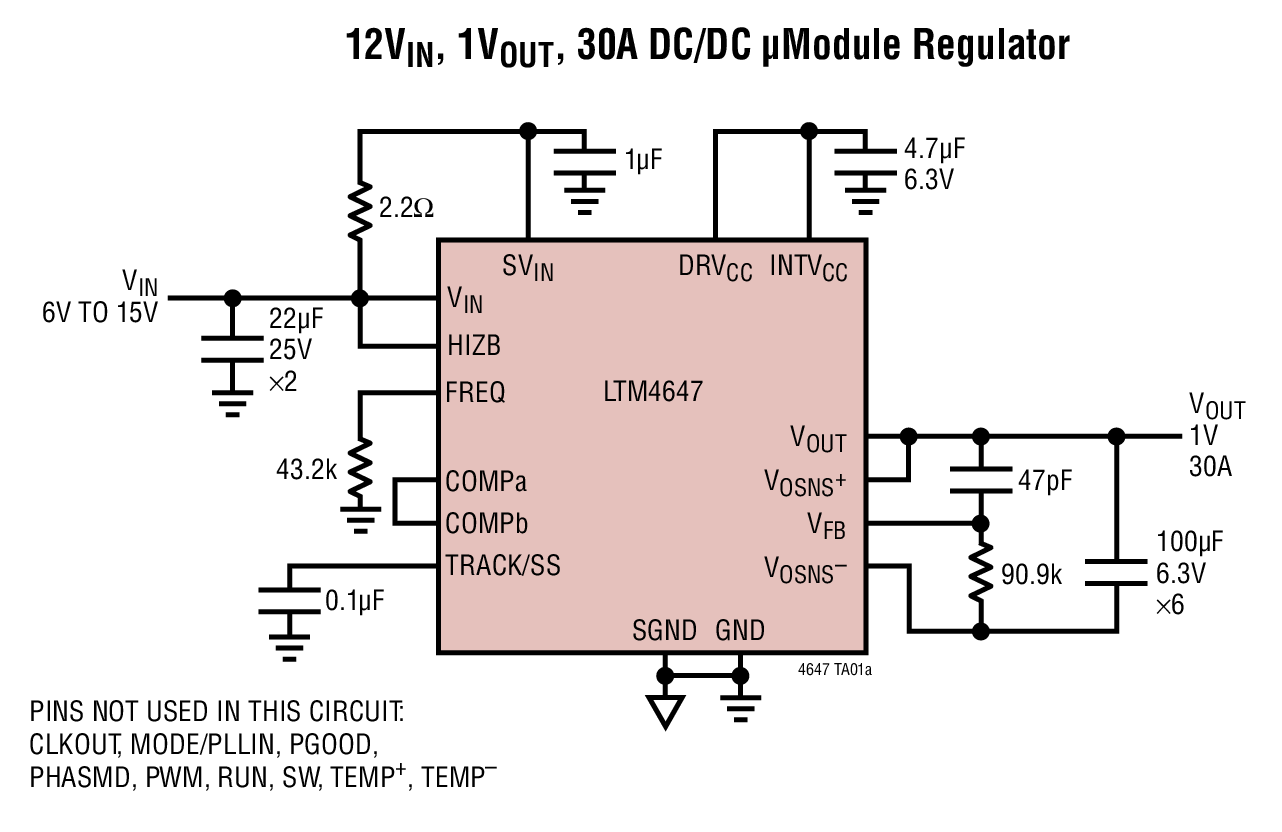
The LTM4647 is a complete 30A output switching mode step-down DC/DC ?Module? (power module) regulator. Included in the package are the switching controller, power FETs, inductor and all supporting components. Operating over an input voltage range of 4.7V to 15V, the LTM4647 supports an output voltage range of 0.6V to 1.8V, set by a single external resistor. Only a few input and output capacitors are needed.Its high efficiency design delivers 87% efficiency from 12V input to 1.0V output with 30A continuous load current. High switching frequency and a current-mode architecture enable a very fast transient response to line and load changes without sacrificing stability. The device supports frequency synchronization, programmable multiphase operation, N+1 phase redundancy, and output voltage tracking for supply rail sequencing.Fault protection features include overvoltage and overcurrent protection. The power module is offered in a space saving 9mm ? 15mm ? 5.01mm BGA package. The LTM4647 is available with SnPb (BGA) or RoHS compliant terminal finish.Applications Telecom, Networking and Industrial Equipment Point of Load Regulation
LTC2372-16 Demo Board | 16-Bit, 500ksps, 8-Channel SAR ADC with 96dB SNR (Requires DC590, DC2026 or DC890)
Analog Devices Inc.
LTC2372-16 Demo Board | 16-Bit, 500ksps, 8-Channel SAR ADC with 96dB SNR (Requires DC590, DC2026 or DC890)
Analog Devices Inc.
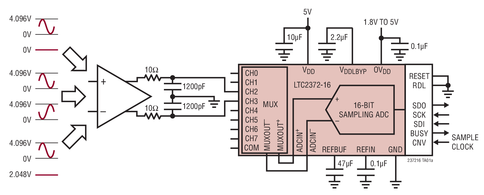
Demonstration circuit 2071A features the LTC2373 family. The LTC2374/LTC2373/LTC2372 are low noise, high speed, 8-channel, 16/18-bit successive approximation register (SAR) ADCs. The demo manual refers to the LTC2373-18 but applies to all parts in the family, the only differences being the number of bits and the maximum sample rate. Operating from a single 5V supply, the LTC2373-18 has a highly configurable, low crosstalk, 8-channel input multiplexer, supporting fully differential, pseudo-differential unipolar and pseudo-differential bipolar analog input ranges.
ADL5317-EVALZ

Analog Devices Inc.
ADL5317-EVALZ
Analog Devices Inc.
The ADL5317 is a high-voltage, wide dynamic range biasing and current monitoring device optimized for use with avalanche photodiodes. With the provision of a stable high-voltage supply up to 80 V, the bias voltage at the VAPD pin can be varied from 6 V to 75 V using the 3 V compatible VSET pin. The current sourced from the VAPD pin, over a range of 5 nA to 5 mA, is accurately mirrored with an attenuation of 5 and sourced from the IPDM monitor output. In a typical application, the monitor output drives a current-input logarithmic amplifier to produce an output representing the optical power incident upon the photodiode. The photodiode anode may be connected to a high-speed transimpedance amplifier for the extraction of the data stream.A signal of 0.2 V to 2.5 V with respect to ground applied at the VSET pin is amplified by a fixed gain of 30 to produce the 6 V to 75 V bias at Pin VAPD. The accuracy of the bias control interface of the ADL5317 allows for straightforward calibration, thereby maintaining a constant avalanche multiplication factor of the photodiode over temperature. The current monitor output, IPDM, maintains its high linearity vs. photodiode current over the full?range of APD bias voltage. The current ratio of 5:1 remains constant as VSET and VPHV are varied.The ADL5317 also offers a supply tracking mode compatible with adjustable high voltage supplies. The VAPD pin accurately follows 2.0 V below the VPHV supply pin when VSET is tied to a voltage from 3.0 V to 5.5 V (or higher with a current limiting resistor), and the VCLH pin is open.Protection from excessive input current at VAPD as well as excessive die temperature is provided. The voltage at VAPD falls rapidly from its setpoint when the input current exceeds 18 mA nominally. A die temperature in excess of 140?C will cause the bias controller and monitor to shut down until the temperature falls below 120?C. Either overstress condition will trigger a logic low at the FALT pin, an open collector output loaded by an external pull-up to an appropriate logic supply (1 mA max).The ADL5317 is available in a 16-lead LFCSP package and is specified for operation from ?40?C to +85?C.APPLICATIONS Optical power monitoring and biasing in APD systems Wide dynamic range voltage sourcing and current monitoring in high voltage systems

19 to 30Vin 12V@10A Active Clamp Forward Reference Design

Texas Instruments
19 to 30Vin 12V@10A Active Clamp Forward Reference Design
Texas Instruments
This reference design provides an isolated 12V at 10A from a 19V-30V input with greater than 93% efficiency. This design uses the UCC2897A active clamp controller with CSD18532Q5B synchronous rectifiers for an efficient: yet cost effective solution that can operate from a 24VDC input bus.
DC1625A-B

Analog Devices Inc.
DC1625A-B
Analog Devices Inc.
The LTC4227 offers ideal diode-OR and Hot Swap? functions for two power rails by controlling external Nchannel MOSFETs. MOSFETs acting as ideal diodes replace two high power Schottky diodes and the associated heat sinks, saving power and board area. A Hot Swap control MOSFET allows a board to be safely inserted and removed from a live backplane by limiting inrush current. The supply output is also protected against short-circuit faults with a fast acting current limit and internal timed circuit breaker.The LTC4227 regulates the forward voltage drop across the MOSFETs to ensure smooth current transfer from one supply to the other without oscillation. The ideal diodes turn on quickly to reduce the load voltage droop during supply switchover. If the input supply fails or is shorted, a fast turn-off minimizes reverse-current transients.The LTC4227 allows turn-on/off control, and reports fault and power good status for the supply. Part Overcurrent Fault Start-Up Delay LTC4227-1 Latch Off 100ms LTC4227-2 Retry 100ms LTC4227-3 Latch Off 1.6ms LTC4227-4 Retry 1.6ms Applications Redundant Power Supplies and Supply Holdup Computer Systems and Servers Telecom Networks
33Vin to 60Vin; 12Vout @ 30A; Dual-Phase Synchronous Buck Converter

Texas Instruments
33Vin to 60Vin; 12Vout @ 30A; Dual-Phase Synchronous Buck Converter
Texas Instruments
A dual-phase synchronous buck converter accepting an input voltage of 33Vin to 60Vin and providing an output of 12Vout capable of supplying 30A
18V-60V Input: 12V@10A Active Clamp Forward

Texas Instruments
18V-60V Input: 12V@10A Active Clamp Forward
Texas Instruments
This reference design provides 12V at 10A from a wide range 18V-60V telecom input with greater than 93% efficiency. This design uses the UCC2897A active clamp controller with synchronous rectifiers for an efficient: yet cost effective solution that can operate from either a 24VDC or 48VDC input bus.
AD9648-125EBZ

Analog Devices Inc.
AD9648-125EBZ
Analog Devices Inc.
The AD9648 is a monolithic, dual-channel, 1.8 V supply, 14-bit, 105 MSPS/125 MSPS analog-to-digital converter (ADC). It features a high performance sample-and-hold circuit and on-chip voltage reference. The product uses multistage differential pipeline architecture with output error correction logic to provide 14-bit accuracy at 125 MSPS data rates and to guarantee no missing codes over the full operating temperature range.The ADC contains several features designed to maximize flexibility and minimize system cost, such as programmable clock and data alignment and programmable digital test pattern generation. The available digital test patterns include built-in deterministic and pseudorandom patterns, along with custom user-defined test patterns entered via the serial port interface (SPI).A differential clock input controls all internal conversion cycles. An optional duty cycle stabilizer (DCS) compensates for wide variations in the clock duty cycle while maintaining excellent overall ADC performance.The digital output data is presented in offset binary, Gray code, or twos complement format. A data output clock (DCO) is provided for each ADC channel to ensure proper latch timing with receiving logic. Output logic levels of 1.8 V CMOS or LVDS are supported. Output data can also be multiplexed onto a single output bus.The AD9648 is available in a 64-lead RoHS compliant LFCSP and is specified over the industrial temperature range (?40?C to +85?C). Applications Communications Diversity radio systems Multimode digital receivers GSM, EDGE, W-CDMA, LTE, CDMA2000, WiMAX, TD-SCDMA I/Q demodulation systems Smart antenna systems Broadband data applications Battery-powered instruments Hand held scope meters Portable medical imaging Ultrasound Radar/LIDARProduct Highlights The AD9648 operates from a single 1.8 V analog power supply and features a separate digital output driver supply to accommodate 1.8 V CMOS or LVDS logic families. The patented sample-and-hold circuit maintains excellent performance for input frequencies up to 200 MHz and is designed for low cost, low power, and ease of use. A standard serial port interface supports various product features and functions, such as data output formatting, internal clock divider, power-down, DCO/data timing and offset adjustments. The AD9648 is packaged in a 64-lead RoHS compliant LFCSP that is pin compatible with the AD9650/AD9269/AD9268 16-bit ADC?s, the AD9258 14-bit ADC, the AD9628/AD9231 12-bit ADC?s, and the AD9608/AD9204 10-bit ADC?s, enabling a simple migration path between 10-bit and 16-bit converters sampling from 20 MSPS to 125 MSPS.
AD7134 Evaluation Board
Analog Devices Inc.
AD7134 Evaluation Board
Analog Devices Inc.
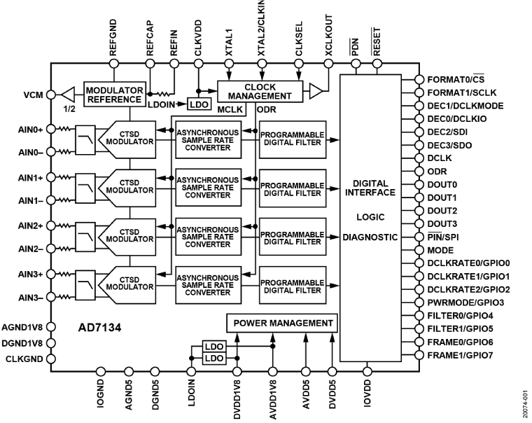
The EVAL-AD7134FMCZ evaluation kit features the AD7134 24-bit, 4-channel, simultaneous sampling, 1.5 MSPS precision alias free analog-to-digital converter (ADC). Two on-board AD7134 ADCs are included to demonstrate multidevice simultaneous sampling. The EVAL-AD7134FMCZ draws power from the system demonstration platform (SDP) EVAL-SDP-CH1Z (SDP-H1) board, and the on-board dc-to-dc regulators regulate an external supply of 8 V to 14 V down to 5 V, 1.8 V, and 1.2 V to supply the AD7134 and peripheral components. Both on-board ADCs have a separate reference of 4.096 V generated by the on-board ADR444. The ADCs have three clock input options and can be clocked by a crystal input, a microelectromechanical system (MEMS) oscillator, or a complementary metal-oxide semiconductor (CMOS) clock. The EVAL-AD7134FMCZ connects to the PC USB port via the SDP-H1 board. The AD7134 evaluation software running on a PC provides full accessibility to the AD7134 device register map, as well as a data analysis interface to display key parameters and graphics from the conversion result in both time and frequency domains. For full details on the AD7134, see the AD7134 data sheet, which must be consulted in conjunction with this user guide when using the EVAL-AD7134FMCZ.
Integrated Gate Driver for Residential Inverters Reference Design

Texas Instruments
Integrated Gate Driver for Residential Inverters Reference Design
Texas Instruments
The PMP9455 reference design provides a highly integrated gate driver solution for 800VA to 3kVA iPure Sine Wave Low Frequency Inverter application . With its unique features of higher peak current drive capability along with integration of two transconductance amplifier with external programmable gain and filtering : the design is a perfect fit for industrial applications . The daughter card design of SM72295 can also be used in various other four switch power topologies such as Buck Boost: Interleaved Buck etc. The Reference design has also been successfully tested on Solar MPPT charger : the details of which can also be found in TIDA-00120 design (http://www.ti.com/tool/TIDA-00120).
LTC3851AUED Demo Board with Adjustable ILIMIT | 4.5V ≤ VIN ≤ 14V, VOUT = 1.5V @ 15A

Analog Devices Inc.
LTC3851AUED Demo Board with Adjustable ILIMIT | 4.5V ≤ VIN ≤ 14V, VOUT = 1.5V @ 15A
Analog Devices Inc.
Demonstration circuit 1432A is a synchronous buck controller featuring the LTC3851AEUD/LTC3851AEUD-1. It operates with an input voltage from 4.5V to 14V and provides 1.5V at up to 15A at the output. The demo circuit is available in two versions. DC1432A-A is configured with LTC3851AEUD which provides ISET function, while the DC1432A-B is configured with LTC3851AEUD-1 which provides PGOOD function.
TMS320VC5409 Bootloader Technical Reference (Rev. A)

Texas Instruments
TMS320VC5409 Bootloader Technical Reference (Rev. A)
Texas Instruments
This document describes the features and operation of the TMS320VC5409 bootloader. The contents of the on-chip ROM also are discussed.**Important Notice Regarding Bootloader Program Contents:**Texas Instruments may periodically update the bootloader code supplied in the ROM to correct known problems provide additional features or improve functionality. These changes may be made without
LTC4012CUF Demo Board | Multi-Chemistry 8A Buck Battery Charger with PowerPath Control

Analog Devices Inc.
LTC4012CUF Demo Board | Multi-Chemistry 8A Buck Battery Charger with PowerPath Control
Analog Devices Inc.
Demonstration circuit 1614 features the LTC4012CUF, a multi-chemistry single battery charger controller with PowerPath™ control. The input supply voltage is 13.5V to 20V and is initially configured for a current limit of 10A. The charger float voltage is programmed by jumpers to support 1- to 4- series cells of both Li-Ion/Polymer and Li-iron phosphate (LiFePO4) at 4.2V/cell and 3.6V/cell, for a total of eight settings. The demo board is initially configured for constant-voltage charging of a 12.6V Li-Ion/ Polymer battery and constant-current charging at 8A, though current derating may be necessary due to certain operating conditions.
EVAL-AD7405FMCZ

Analog Devices Inc.
EVAL-AD7405FMCZ
Analog Devices Inc.
The AD7405 is a high performance, second-order, ?-? modulatorthat converts an analog input signal into a high speed, single-bitLVDS data stream, with on-chip digital isolation based onAnalog Devices, Inc., iCoupler? technology. The AD7405operates from a 5 V (VDD1) power supply and accepts adifferential input signal of ?250 mV (?320 mV full-scale). Thedifferential input is ideally suited to shunt voltage monitoring inhigh voltage applications where galvanic isolation is required.The analog input is continuously sampled by a high performanceanalog modulator, and converted to a ones density digital outputstream with a data rate of up to 20 MHz. The originalinformation can be reconstructed with an appropriate digitalfilter to achieve 88 dB signal to noise ratio (SNR) at 78.1 kSPS.The LVDS input/output can use a 5 V or a 3.3 V supply (VDD2).The LVDS interface is digitally isolated. The LVDS interfacetechnology, combined with monolithic transformer technology,means the on-chip isolation provides outstanding performancecharacteristics, superior to alternatives such as optocouplerdevices. The AD7405 device is offered in a 16-lead, wide-bodySOIC package and has an operating temperature range of ?40?Cto +125?C.Applications Shunt current monitoring AC motor controls Power and solar inverters Wind turbine inverters Data acquisition systems Analog-to-digital and opto-isolator replacements