Search results
ADL5390-EVALZ

Analog Devices Inc.
ADL5390-EVALZ
Analog Devices Inc.
The ADL5390 vector multiplier consists of a matched pair of broadband variable gain amplifiers whose outputs are summed. The separate gain controls for each amplifier are linear-in-magnitude. If the two input RF signals are in quadrature, the vector multiplier can be configured as a vector modulator or as a variable attenuator/phase shifter by using the gain control pins as Cartesian variables. In this case, the output amplitude can be controlled from a maximum of +5 dB to less than -30 dB, and the phase can be shifted continuously over the entire 360? range. Since the signal paths are linear, the original modulation on the inputs is preserved. If the two signals are independent, then the vector multiplier can function as a 2:1 multiplexer or can provide fading from one channel to another.The ADL5390 operates over a wide frequency range of 20 MHz to 2400 MHz. For a maximum gain setting on one channel at 380 MHz, the ADL5390 delivers an OP1dB of 11 dBm, an OIP3 of 24 dBm, and an output noise floor of -148 dBm/Hz. The gain and phase matching between the two VGAs is better than 0.5 dB and 1?, respectively, over most of the operating range.The ADL5390 is fabricated on Analog Devices' proprietary, high performance 25 GHz SOI complementary bipolar IC process. It is available in a 24-lead, Pb-free CSP package and operates over a -40?C to +85?C temperature range. Evaluation boards are available.APPLICATIONS PA linearization and predistortion Amplitude and phase modulation Variable matched attenuator and/or phase shifter Cellular base stations Radio links Fixed wireless access Broadband/CATV RF/IF analog multiplexerAVAILABILITYSamples, part number ADL5390ACPZ, and an evaluation board, part number ADL5390-EVAL, are available.COMPANION PRODUCTSAD8302 - LF to 2.7GHz RF/IF Gain Phase DetectorAD8340 - RF Vector Modulator 700MHz to 1000MHzAD8341 - RF Vector Modulator 1.5GHz to 2.4GHz
EVAL-AD7843EBZ

Analog Devices Inc.
EVAL-AD7843EBZ
Analog Devices Inc.
The AD7843 is a 12-bit successive-approximation ADC with a synchronous serial interface and low on resistance switches for driving touch screens. The part operates from a single 2.2 V to 5.25 V power supply and features throughput rates greater than 125 kSPS. The external reference applied to the AD7843 can be varied from 1 V to +VCC, while the analog input range is from 0 V to VREF. The device includes a shutdown mode that reduces the current consumption to less than 1 ?A. This part is available in a 16-lead 0.15' Quarter Size Outline (QSOP) package and a 16-lead Thin Shrink Small Outline (TSSOP) package.?Also see the AD7843 sister part, which is the AD7873. This part is similar to the AD7843 but has added functionality such as an on-chip temperature sensor (-40?C to + 85?C), on-chip 2.5 V reference and direct battery and touch-pressure measurement.
ADP5071CP-EVALZ

Analog Devices Inc.
ADP5071CP-EVALZ
Analog Devices Inc.
The ADP5071 is a dual high performance dc-to-dc regulator that generates independently regulated positive and negative rails.The input voltage range of 2.85 V to 15 V supports a wide variety of applications. The integrated main switch in both regulators enables generation of an adjustable positive output voltage up to +39 V and a negative output voltage down to ?39 V below input voltage.The ADP5071 operates at a pin selected 1.2 MHz/2.4 MHz switching frequency. The ADP5071 can synchronize with an external oscillator from 1.0 MHz to 2.6 MHz to ease noise filtering in sensitive applications. Both regulators implement programmable slew rate control circuitry for the MOSFET driver stage to reduce electromagnetic interference (EMI).Flexible start-up sequencing is provided with the options of manual enable, simultaneous mode, positive supply first, and negative supply first.The ADP5071 includes a fixed internal or resistor programmable soft start timer to prevent inrush current at power-up. During shutdown, both regulators completely disconnect the loads from the input supply to provide a true shutdown.Other key safety features in the ADP5071 include overcurrent protection (OCP), overvoltage protection (OVP), thermal shutdown (TSD), and input undervoltage lockout (UVLO).The ADP5071 is available in a 20-lead LFCSP or in a 20-lead TSSOP and is rated for a ?40?C to +125?C junction temperature range.Applications Bipolar amplifiers, ADCs, DACs, and multiplexers Charge-coupled device (CCD) bias supply Optical module supply RF power amplifier (PA) bias
ADMV1012-EVALZ

Analog Devices Inc.
ADMV1012-EVALZ
Analog Devices Inc.
The ADMV1012 is a compact, gallium arsenide (GaAs) design, monolithic microwave integrated circuit (MMIC) double sideband (DSB) downconverter in a RoHS compliant package optimized for point to point microwave radio designs that operate in the 17.5 GHz to 24 GHz input frequency range. The ADMV1012 provides 15 dB of conversion gain with 25 dB of image rejection, and 2.5 dB noise figure. The ADMV1012 uses a radio frequency (RF) low noise amplifier (LNA) followed by an in phase/quadrature (I/Q), double balanced mixer, where a driver amplifier drives the local oscillator (LO) with a ?2 multiplier. IF1 and IF2 mixer quadrature outputs are provided, and an external 90? hybrid is required to select the required sideband.The I/Q mixer topology reduces the need for filtering of unwanted sideband. The ADMV1012 is a much smaller alternative to hybrid style DSB downconverter assemblies and eliminates the need for wire bonding by allowing the use of surface-mount manufacturing assemblies.The ADMV1012 downconverter comes in a compact, thermally enhanced, 4.9 mm ? 4.9 mm, 32-terminal LCC. The ADMV1012 operates over the ?40?C to +85?C temperature range.Applications Point to point microwave radios Radars and electronic warfare systems Instrumentation, automatic test equipment (ATE)Satellite communications
Direct Type/ Local Dimming (Conventional TV power + Boost + LED driver)

Texas Instruments
Direct Type/ Local Dimming (Conventional TV power + Boost + LED driver)
Texas Instruments
In this topology: the UCC28051 is a boost transition mode (TM) power factor corrector (PFC): which can rectify an AC input line voltage to 380V DC; the resonant LLC stage UCC25600 regulates the output to 24V/2A for an audio amplifier with feedback to the LLC controller: and 48V for the LED driver input. The flyback with UCC28610 in parallel generates 5V/3A for the system board and 5V/1A for standby power. In the LED driver stage: the 48V input voltage requires another front end boost stage to boost the output voltage to 80V: which connects to the eight-channel TLC5960 with 20LEDs at 120mA per string.This technique is the most common type of current LED backlight; the LLC design is easily implemented. The intelligent headroom voltage monitor (oriHVM™) automatically minimizes the power loss caused by the LED forward voltage change. Only a single additional resistor regulates the boost dc-dc output voltage.
DC1893A
Analog Devices Inc.
DC1893A
Analog Devices Inc.
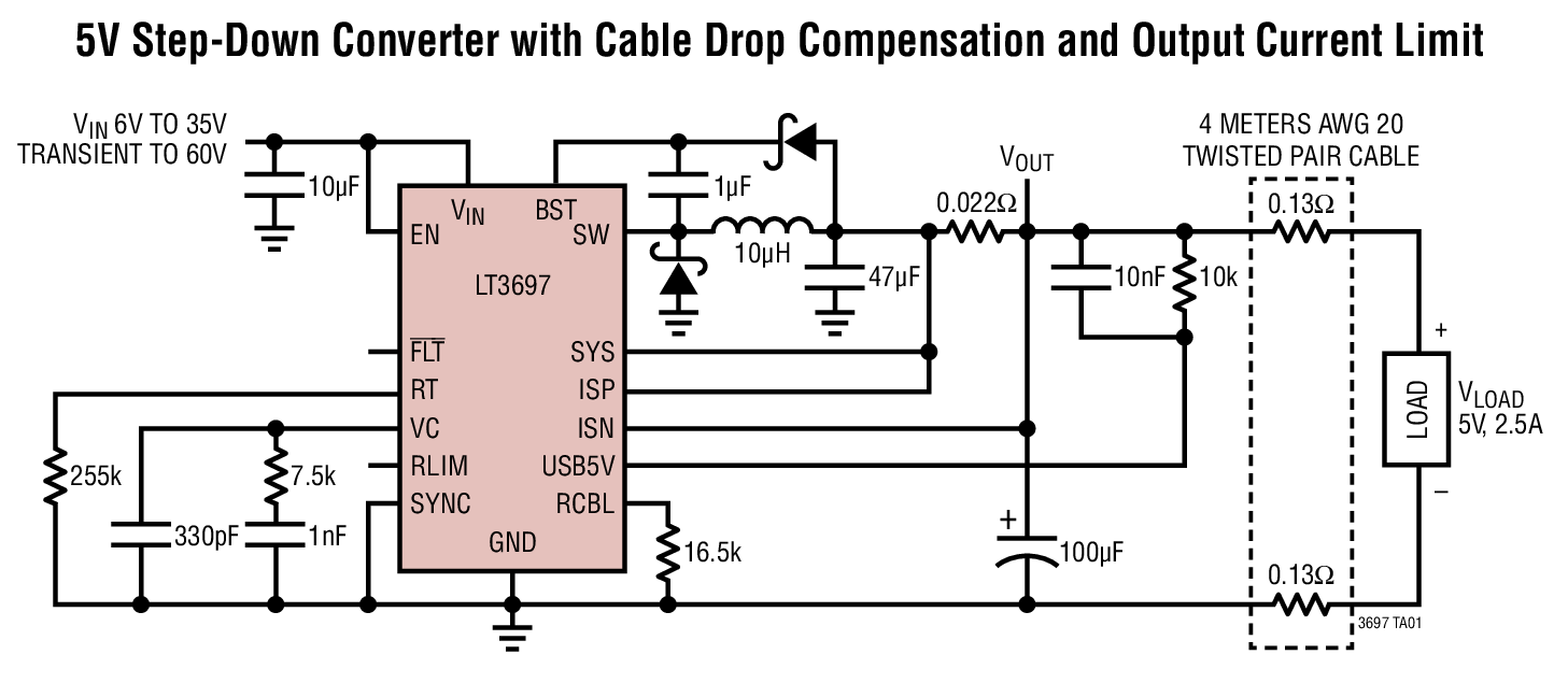
The LT3697 is a 35V, 2.5A step-down switching regulator designed to power 5V USB applications. A precise output voltage and programmable cable drop compensation maintain accurate 5V regulation at the USB socket connected to the end of a long cable. The accurate, programmable current limit can eliminate the need for a USB power switch and improve system reliability. The provided 180mA active load reduces output overshoot during load transients. Dual feedback allows regulation on the output of a USB switch and limits cable drop compensation to a maximum of 6.1V output, protecting USB devices during fault conditions. A separate 5V output can be taken from the SYS terminal to power auxiliary circuitry such as a USB hub controller. The LT3697 also provides a load current monitor output and an overcurrent fault indicator.The LT3697 operates from 300kHz to 2.2MHz and withstands input voltage transients up to 60V. The device's output survives shorts to ground and to the battery. A current mode topology is used for fast transient response and good loop stability. Shutdown reduces input supply current to less than 1?A. The LT3697 is available in a 16-lead MSOP package with an exposed pad for low thermal resistance.Applications Automotive USB Industrial USB
ADM7171CP-EVALZ

Analog Devices Inc.
ADM7171CP-EVALZ
Analog Devices Inc.
The ADM7171 is a CMOS, low dropout linear regulator (LDO) that operates from 2.3 V to 6.5 V and provides up to 1 A of output current. This high output current LDO is ideal for regulation of high performance analog and mixed signal circuits operating from 6 V down to 1.2 V rails. Using an advanced proprietary architecture, the device provides high power supply rejection and low noise, and achieves excellent line and load transient response with just a small 4.7 ?F ceramic output capacitor. Load transient response is typically 1.5 ?s for a 1 mA to 500 mA load step.The ADM7171 is available in 17 fixed output voltage options. The following voltages are available from stock: 1.3 V, 1.8 V, 2.5 V, 3.0 V, 3.3 V, 4.2 V, and 5.0 V. Additional voltages that are available by special order are: 1.5 V, 1.85 V, 2.0 V, 2.2 V, 2.7 V, 2.75 V, 2.8 V, 2.85 V, 3.8 V, and 4.6 V. An adjustable version is also available that allows output voltages that range from 1.2 V to VIN ? VDO with an external feedback divider.Inrush current can be controlled by adjusting the start-up time via the soft start pin. The typical start-up time with a 1 nF soft start capacitor is 1.0 ms.The ADM7171 regulator output noise is 5 ?V rms independent of the output voltage. The ADM7171 is available in an 8-lead, 3 mm ? 3 mm LFCSP, making it not only a very compact solution, but also providing excellent thermal performance for applications requiring up to 1 A of output current in a small, low profile footprint.Applications Regulation to noise sensitive applications: ADC and DAC circuits, precision amplifiers, PLLs/VCOs, and clocking ICs Communications and infrastructure Medical and healthcare Industrial and instrumentation
AD7134 Evaluation Board
Analog Devices Inc.
AD7134 Evaluation Board
Analog Devices Inc.
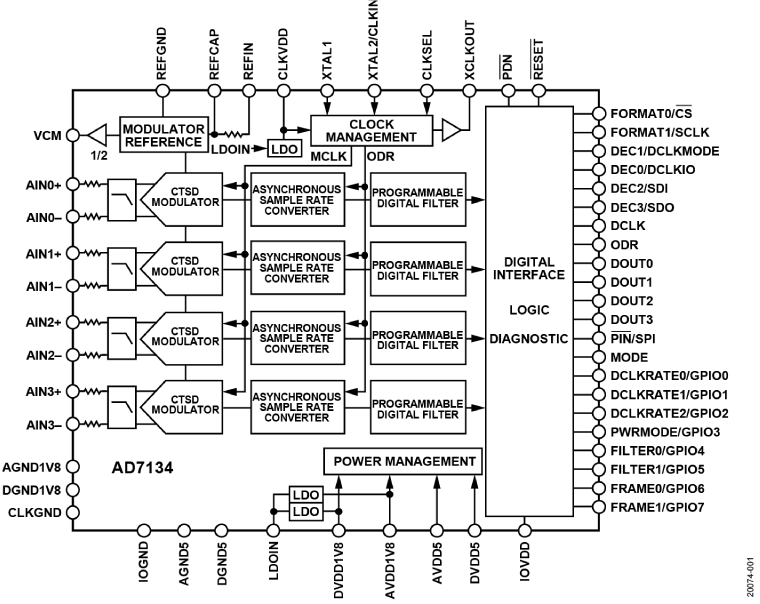
The EVAL-AD7134FMCZ evaluation kit features the AD7134 24-bit, 4-channel, simultaneous sampling, 1.5 MSPS precision alias free analog-to-digital converter (ADC). Two on-board AD7134 ADCs are included to demonstrate multidevice simultaneous sampling. The EVAL-AD7134FMCZ draws power from the system demonstration platform (SDP) EVAL-SDP-CH1Z (SDP-H1) board, and the on-board dc-to-dc regulators regulate an external supply of 8 V to 14 V down to 5 V, 1.8 V, and 1.2 V to supply the AD7134 and peripheral components. Both on-board ADCs have a separate reference of 4.096 V generated by the on-board ADR444. The ADCs have three clock input options and can be clocked by a crystal input, a microelectromechanical system (MEMS) oscillator, or a complementary metal-oxide semiconductor (CMOS) clock. The EVAL-AD7134FMCZ connects to the PC USB port via the SDP-H1 board. The AD7134 evaluation software running on a PC provides full accessibility to the AD7134 device register map, as well as a data analysis interface to display key parameters and graphics from the conversion result in both time and frequency domains. For full details on the AD7134, see the AD7134 data sheet, which must be consulted in conjunction with this user guide when using the EVAL-AD7134FMCZ.
Advanced Profiling with XDS560 Trace (Rev. A)

Texas Instruments
Advanced Profiling with XDS560 Trace (Rev. A)
Texas Instruments
While many developers consider XDS560 Trace a valuable tool for debugging difficult scenarios it also provides quick and effective profiling techniques. With the capability of Trace to capture timestamps on each sample and the flexibility of Advanced Event Triggering to capture data at the appropriate locations XDS560 Trace provides unique profiling capabilities. This application note focuses on
Security Tracker in Automotive Applications

Texas Instruments
Security Tracker in Automotive Applications
Texas Instruments
This reference design supports the supply for a security tracker using the TPS40200-Q1: with the opportunity of a wide input voltage range from 8V-50V. The output can handle 4.3V up to 3A due to the non-synchronous buck controller. The reference design also allows for flexible design with a simple configuration due to the device.
ADM1270RQ-EVALZ

Analog Devices Inc.
ADM1270RQ-EVALZ
Analog Devices Inc.
The ADM1270 is a current-limiting controller that providesinrush current limiting and overcurrent protection for modularor battery-powered systems. When circuit boards are insertedinto a live backplane, discharged supply bypass capacitors drawlarge transient currents from the backplane power bus as theycharge. These transient currents can cause permanent damageto connector pins, as well as dips on the backplane supply thatcan reset other boards in the system.The ADM1270 is designed to control the inrush current, whenpowering on the system, via an external P-channel field effecttransistor (FET).To protect the system from a reverse polarity input supply, thereis a provision made to control an additional external P-channelFET. This feature prevents reverse current flow in case of a reversepolarity connection, which can damage the load or the ADM1270.The ADM1270 is available in a 3 mm ? 3 mm, 16-lead LFCSP anda 16-lead QSOP. Applications Industrial modules Battery-powered/portable instrumentation