
Search results
EVAL-ADAQ4001FMCZ

Analog Devices Inc.
EVAL-ADAQ4001FMCZ
Analog Devices Inc.
The ADAQ4001 is a ?Module? precision data acquisition (DAQ), signal chain solution that reduces the development cycle of a precision measurement system by transferring the signal chain design challenge of component selection, optimization, and layout from the designer to the device. Using system-in-package (SIP) technology, the ADAQ4001 reduces end system component count by combining multiple common signal processing and conditioning blocks into a single device. These blocks include a high resolution 16-bit, 2 MSPS successive approximation register (SAR), analog-to-digital converter (ADC), a low noise, fully differential ADC driver amplifier (FDA), and a stable reference buffer. Using Analog Devices, Inc., iPassives? technology, the ADAQ4001 also incorporates crucial passive components with superior matching and drift characteristics to minimize temperature dependent error sources and to offer optimized performance (see Figure 1 in the data sheet). Housing this signal chain solution in a small, 7 mm ? 7 mm, 0.80 mm pitch, 49-ball CSP_BGA enables compact form factor designs without sacrificing performance and simplifies end system bill of materials management. This level of system integration makes the ADAQ4001 much less sensitive to printed circuit board (PCB) layout while still providing flexibility to adapt to a wide range of signal levels. The serial peripheral interface (SPI)-compatible, serial user interface is compatible with 1.8 V, 2.5 V, 3 V, or 5 V logic, using a separate VIO supply. Specified operation of the ADAQ4001 is from ?40?C to +125?C.APPLICATIONSAutomatic test equipmentMachine automationProcess controlsMedical instrumentationDigital control loops
Respiration Rate Measurement Using Impedance Pneumography

Texas Instruments
Respiration Rate Measurement Using Impedance Pneumography
Texas Instruments
This document discusses the use of impedance pneumography as a technique to measure respiration rate. The generation of high-frequency ac current source is described and the issues related to delay in modulated signal and finite transition times of carriers are addressed. The report also includesdescriptions of potential implementations of a respiration rate measurement system using the ADS1298
Qi (WPC) Compliant Wireless Charger for Low Power Wearable Applications

Texas Instruments
Qi (WPC) Compliant Wireless Charger for Low Power Wearable Applications
Texas Instruments
TI design TIDA-00318 is suitable for low power wearable device including a Qi compliant wireless receiver (bq51003)and ultra low current 1 cell Li-ion linear charger (bq25100). It features an ultra small size (5x15mm2), capable of low charging currents down to 10mA and up to 250mAwith support of termination currents as low as 1mA. Current design is designed for 135mA charge current application.
Single-Ended Input to Differential Output Conversion Circuit Reference Design

Texas Instruments
Single-Ended Input to Differential Output Conversion Circuit Reference Design
Texas Instruments
This TI Precision Verified Design provides the theory: component selection: simulation: PCB design: and measurement details for a single ended input to differential output circuit which converts a single ended input of +0.1V to +2.4V into a differential output of ± 2.3V on a single +2.7V supply. The output range is intentionally limited to maximize linearity. The circuit is composed of 2 amplifiers. One amplifier acts as a buffer and creates a voltage: Vout+. The second amplifier inverts the input and adds a reference voltage to generate Vout-. Both Vout+ and Vout- range from 0.1V to 2.4V. The difference: Vdiff: is the difference between Vout+ and Vout-. This makes the differential output voltage range +2.3V.
Primary-Side Regulated Flyback with 85-265VAC Input (24V @ 1.7A) Reference Design

Texas Instruments
Primary-Side Regulated Flyback with 85-265VAC Input (24V @ 1.7A) Reference Design
Texas Instruments
The PMP9041 reference design uses the UCC28710 primary-side regulated flyback controller to generate a 24V/40W output from a univeral AC input. The valley switching of the UCC28710 allows this low-cost design to achieve a maximum load efficiency of 90%; no load losses are less than 50mW.
Using Advanced Event Triggering to Debug Real-Time Problems in Embedded Systems
Texas Instruments
Using Advanced Event Triggering to Debug Real-Time Problems in Embedded Systems
Texas Instruments
As more and more system components become embedded within the system processor chip new techniques are required for debug. Signals and busses that were historically available for probe connection at external package pins are now hidden from the users within the processor package. This problem is referred to as vanishing visibility meaning that the user can no longer employ traditional techniques
LTC3639EMSE Demo Board | Sync Buck, 4V ≤ VIN ≤ 150V, VOUT = 1.8V/3.3V/5V/Adj @ 100mA
Analog Devices Inc.
LTC3639EMSE Demo Board | Sync Buck, 4V ≤ VIN ≤ 150V, VOUT = 1.8V/3.3V/5V/Adj @ 100mA
Analog Devices Inc.
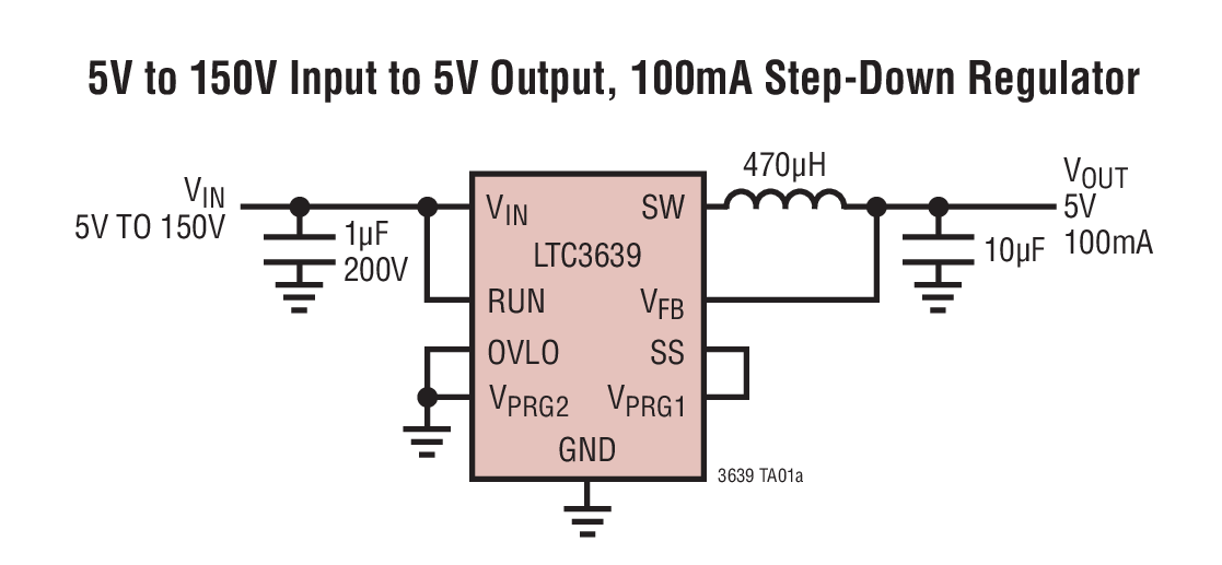
Demonstration circuit 1901A is a 150V input, 100mA output DC/DC power supply featuring the LTC3639. The IC operates in a high efficiency Burst Mode® operation and includes internal high and low side power MOSFETs. The board will accept an input voltage between 4V and 150V, and provide jumper selected output voltages of 1.8V, 3.3V, 5V and an option for additional voltages. The IC includes internal soft-start and a provision for increasing soft-start time.
300VDC-800VDC Input: 54W 4 Channel Outputs: PSR Flyback with SiC-FET Reference Design

Texas Instruments
300VDC-800VDC Input: 54W 4 Channel Outputs: PSR Flyback with SiC-FET Reference Design
Texas Instruments
This design uses low cost primary side regulation (PSR) IC UCC28700 with a SiC-FET for 300VDC-800VDC input range. Four outputs with separated grounds: 25V/19W: 25V/17W: 25V/10.1W: and 25V/8W are generated.

EV-ADF4155EB1Z

Analog Devices Inc.
EV-ADF4155EB1Z
Analog Devices Inc.
The ADF4155 allows implementation of fractional-N or integer-N phase-locked loop (PLL) frequency synthesizers when used with an external loop filter, external voltage controlled oscillator (VCO), and external reference frequency.The ADF4155 is for use with external VCO parts up to an 8 GHz operating frequency. The high resolution programmable modulus allows synthesis of exact frequencies with 0 Hz error.The VCO frequency can be divided by 1, 2, 4, 8, 16, 32, or 64 to allow the user to generate RF output frequencies as low as 7.8125 MHz.Control of all on-chip registers is through a simple 3-wire interface. The device operates with a nominal power supply of 3.3 V ? 5% and can be powered down when not in use.The ADF4155 is available in a 24-lead, 4 mm ? 4 mm LFCSP package.APPLICATIONS Wireless infrastructure (W-CDMA, TD-SCDMA, WiMAX, GSM, PCS, DCS, DECT) Point to point/point to multipoint microwave links Test equipment Wireless LANs, CATV equipment Clock generation

LMZ12010 20VIN 10AOUT Simple Switcher? Module Reference Design

Texas Instruments
LMZ12010 20VIN 10AOUT Simple Switcher? Module Reference Design
Texas Instruments
The LMZ13610/8 and LMZ12010/8 SIMPLE SWITCHER® power modules are easy-to-use DC-DC solution capable of driving up to a 10A load. They are available in an innovative package that enhances thermal performance and allows for hand or machine soldering. The LMZ13610/8 can accept an input voltage rail between 6V and 36V and the LMZ12010/8 can accept an input voltage rail between 6V and 20V. The devices can deliver an adjustable and highly accurate output voltage as low as 0.8V and as high as 6V. The control structure is constant frequency PWM. The control loop operates well with low ESR output capacitors such as ceramics. The precision enable input allows for programmable UVLO of the input supply. The external soft-start capacitor facilitates a controlled and adjustable startup rise time of the output. The LMZ13610 and LMZ12010 family is a reliable and robust solution with the following features: loss-less cycle-by-cycle valley current limit to protect for over current or short-circuit fault, thermal shutdown, input under-voltage lockout, and will start up into a pre-biased output. Free-running switching frequency is 350 kHz.
DC1884A-C

Analog Devices Inc.
DC1884A-C
Analog Devices Inc.
The LTM9011-14/LTM9010-14/LTM9009-14 are 8-channel, simultaneous sampling 14-bit A/D converters designed for digitizing high frequency, wide dynamic range signals. AC performance includes 73.1dB SNR and 88dB spurious free dynamic range (SFDR). Low power consumption per channel reduces heat in high channel count applications. Integrated bypass capacitance and flow-through pinout reduces overall board space requirements.DC specs include ?1LSB INL (typ), ?0.3LSB DNL (typ) and no missing codes over temperature. The transition noise is a low 1.2LSBRMS.The digital outputs are serial LVDS to minimize the number of data lines. Each channel outputs two bits at a time (2-lane mode). At lower sampling rates there is a one bit per channel option (1-lane mode).The ENC+ and ENC? inputs may be driven differentially or single-ended with a sine wave, PECL, LVDS, TTL, or CMOS inputs. An internal clock duty cycle stabilizer allows high performance at full speed for a wide range of clock duty cycles.Applications Communications Cellular Base Stations Software Defined Radios Portable Medical Imaging Multichannel Data Acquisition Nondestructive Testing
EV1HMC8364LP6G

Analog Devices Inc.
EV1HMC8364LP6G
Analog Devices Inc.
The HMC8364 is a gallium arsenide (GaAs), quadband, monolithic microwave integrated circuit (MMIC), voltage controlled oscillator (VCO) designed to offer wideband frequency capabilities without compromising phase noise performance. The device integrates four independent, narrow-band VCOs with overlapping frequency bands, operating at a fundamental frequency range of 18.10 GHz to 26.60 GHz. The consistent tuning sensitivity across all frequency bands simplifies the synthesizer loop filter design.The tuning port is common to all VCO cores for a simpler design of the phase-locked loop (PLL) feedback path. The HMC8364 also offers a low typical current consumption of 99 mA for power sensitive applications. The HMC8364 integrates resonators, negative resistance devices, and varactor diodes. The monolithic structure of the oscillator offers very low phase noise, optimal temperature stability, and is immune to vibration and process variation.The four VCOs are packaged in a single, 6 mm ? 6 mm, surface-mount lead frame chip scale package (LFCSP), and require no external matching components. Combined with a high frequency, high performance PLL, the ADF41513, the HMC8364 offers a complete RF or microwave frequency generation solution.APPLICATIONS Electronic test and measurement Industrial and medical instrumentation Point to point and multipoint radios Aerospace and defense Wireless communication infrastructure