
Search results
LT3754EUH Demo Board | 16-Channel Boost LED Driver, 20V ≤ VIN ≤ 28V, VLED = 55V @ 50mA

Analog Devices Inc.
LT3754EUH Demo Board | 16-Channel Boost LED Driver, 20V ≤ VIN ≤ 28V, VLED = 55V @ 50mA
Analog Devices Inc.
DC1436A is a 16-Channel High Voltage Boost LED Driver featuring the LT3754. The LT3754 drives up to 50mA per string and has a maximum LED string voltage of 45V. The VIN terminal is powered from an 8V to 14V input supply and is distinct from the 24V PVIN supply (20V to 28V) for best thermal performance. Overvoltage protection is set at 55V in case the LEDs are removed from the circuit. If the LEDs are opened, the FAULT terminal output flag goes low and reports the fault condition. If one or more of the 16 LED channels is not used, its LED pin or terminal should be tied to VOUT (LED+) to disable it. Multiple channels can be tied in parallel by tying their LED1-LED16 pins together.
EV1HMC8364LP6G

Analog Devices Inc.
EV1HMC8364LP6G
Analog Devices Inc.
The HMC8364 is a gallium arsenide (GaAs), quadband, monolithic microwave integrated circuit (MMIC), voltage controlled oscillator (VCO) designed to offer wideband frequency capabilities without compromising phase noise performance. The device integrates four independent, narrow-band VCOs with overlapping frequency bands, operating at a fundamental frequency range of 18.10 GHz to 26.60 GHz. The consistent tuning sensitivity across all frequency bands simplifies the synthesizer loop filter design.The tuning port is common to all VCO cores for a simpler design of the phase-locked loop (PLL) feedback path. The HMC8364 also offers a low typical current consumption of 99 mA for power sensitive applications. The HMC8364 integrates resonators, negative resistance devices, and varactor diodes. The monolithic structure of the oscillator offers very low phase noise, optimal temperature stability, and is immune to vibration and process variation.The four VCOs are packaged in a single, 6 mm ? 6 mm, surface-mount lead frame chip scale package (LFCSP), and require no external matching components. Combined with a high frequency, high performance PLL, the ADF41513, the HMC8364 offers a complete RF or microwave frequency generation solution.APPLICATIONS Electronic test and measurement Industrial and medical instrumentation Point to point and multipoint radios Aerospace and defense Wireless communication infrastructure
What is a .tmap File? (Rev. A)

Texas Instruments
What is a .tmap File? (Rev. A)
Texas Instruments
The PowerLAN™ Master Gateway Battery Management Controller uses a file identified by the .tmap file extension to load configuration parameters. This file serves to configure the operation of the controller to the specific application. Examples of configurable parameters are number of parallel and series cells in the pack number of temperature sensors and state-of-charge indication (SOCi) dis
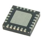
SI53362-B-GM
Silicon Laboratories (Silicon Labs)
From $1.15 • 100+ units available from Mouser Electronics
| Distributor | SKU | Stock | MOQ | 1 | 10 | 50 | 100 | 1,000 | 10,000 | |
|---|---|---|---|---|---|---|---|---|---|---|
| DigiKey | SI53362-B-GMR-ND | 0 | 1,000 | $1.61 | $1.61 | $1.47 | $1.34 | $1.20 | $1.20 | |
| Mouser Electronics | 634-SI53362-B-GM | 755 | 1 | $1.55 | $1.45 | $1.37 | $1.29 | $1.15 | $1.15 | |
| AVNET Europe | SI53362-B-GM | 0 | 1 | $1.29 | $1.28 | $1.24 | $1.22 | $1.22 | $1.22 | Buy |
| Arrow North American Components | SI53362-B-GM | 0 | 490 | $1.53 | $1.50 |
EVAL-AD5940ELCZ

Analog Devices Inc.
EVAL-AD5940ELCZ
Analog Devices Inc.
The AD5940 and AD5941 are high precision, low power analog front ends (AFEs) designed for portable applications that require high precision, electrochemical-based measurement techniques, such as amperometric, voltammetric, or impedance measurements. The AD5940/AD5941 is designed for skin impedance and body impedance measurements, and works with the AD8233 AFE in a complete bioelectric or biopotential measurement system. The AD5940/AD5941 is designed for electrochemical toxic gas sensing.The AD5940/AD5941 consist of two high precision excitation loops and one common measurement channel, which enables a wide capability of measurements of the sensor under test. The first excitation loop consists of an ultra low power, dual-output string, digital-to-analog converter (DAC), and a low power, low noise potentiostat. One output of the DAC controls the noninverting input of the potentiostat, and the other output controls the noninverting input of the transimpedance amplifier (TIA). This low power excitation loop is capable of generating signals from dc to 200 Hz.The second excitation loop consists of a 12-bit DAC, referred to as the high speed DAC. This DAC is capable of generating high frequency excitation signals up to 200 kHz.The AD5940/AD5941 measurement channel features a 16-bit, 800 kSPS, multichannel successive approximation register (SAR) analog-to-digital converter (ADC) with input buffers, a built in antialias filter, and a programmable gain amplifier (PGA). An input multiplexer (mux) in front of the ADC allows the user to select an input channel for measurement. These input channels include multiple external current inputs, external voltage inputs, and internal channels. The internal channels allow diagnostic measurements of the internal supply voltages, die temperature, and reference voltages.The current inputs include two TIAs with programmable gain and load resistors for measuring different sensor types. The first TIA, referred to as the low power TIA, measures low bandwidth signals. The second TIA, referred to as the high speed TIA, measures high bandwidth signals up to 200 kHz.An ultra low leakage, programmable switch matrix connects the sensor to the internal analog excitation and measurement blocks. This matrix provides an interface for connecting external transimpedance amplifier resistors (RTIAs) and calibration resistors. The matrix can also be used to multiplex multiple electronic measurement devices to the same wearable electrodes.A precision 1.82 V and 2.5 V on-chip reference source is available. The internal ADC and DAC circuits use this on-chip reference source to ensure low drift performance for the 1.82 V and 2.5 V peripherals.The AD5940/AD5941 measurement blocks can be controlled via direct register writes through the serial peripheral interface (SPI) interface, or, alternatively, by using a preprogrammable sequencer, which provides autonomous control of the AFE chip. 6 kB of static random access memory (SRAM) is partitioned for a deep data first in, first out (FIFO) and command FIFO. Measurement commands are stored in the command FIFO and measurement results are stored in the data FIFO. A number of FIFO related interrupts are available to indicate when the FIFO is full.A number of general-purpose inputs/outputs (GPIOs) are available and controlled using the AFE sequencer. The AFE sequencer allows cycle accurate control of multiple external sensor devices.The AD5940/AD5941 operate from a 2.8 V to 3.6 V supply and are specified over a temperature range of ?40?C to +85?C. The AD5940 is packaged in a 56-lead, 3.6 mm ? 4.2 mm WLCSP. The AD5941 is packaged in a 48-lead LFCSP.APPLICATIONS Electrochemical measurements Electrochemical gas sensors Potentiostat/amperometric/voltammetry/cyclic voltammetry Bioimpedance applications Skin impedance Body impedance Continuous glucose monitoring Battery impedance
LTC3855EUJ Demo Board | Dual Output, VIN = 4.5V to 14V, VOUT1 = 1.8V @ 17A, VOUT2 = 1.2V @ 17A

Analog Devices Inc.
LTC3855EUJ Demo Board | Dual Output, VIN = 4.5V to 14V, VOUT1 = 1.8V @ 17A, VOUT2 = 1.2V @ 17A
Analog Devices Inc.
Demonstration circuit DC1441A is a dual output synchronous buck converter featuring the LTC3855EUJ. The board provides two outputs of 1.8V/17A and 1.2V/17A from an input voltage of 4.5V to 14V at a switching frequency of 400kHz.
Digital Video Recorder Reference Designs
Texas Instruments
Digital Video Recorder Reference Designs
Texas Instruments
Texas Instruments offers low-cost: low-power: integrated multichannel reference designs featuring the Hybrid DVR (DVR/NVR) reference design based on the highly integrated TMS320DM816x and TMS320DM8107 DaVinci™ video processors. This single platform solution allows faster development at a reduced cost.DM8107 DVR Reference DesignOrder NowPart number:DM8107DVR-UD1Price:$1095Description:Single platform solution based on the TMS320DM8107 DaVinci video processor provides configurations for 4/8/16 channel DVRs. Provide 1000fps CIF H.264/SVCT encode/decode with integrated HDMI/VGA/CVBS output on a single processor.Processors:New low power: cost optimized DM8107 processor and new TVP5158 multi-channel video decoder with integrated audio. DM8107 includes ARM® Cortex™-A8: SVCT/H.264/MJPEG video coprocessor: Gigabit EMAC: PCIe for BOM savingsHardware:Multi-storage of compressed input (SATA x2 to x8 with support for DVD backup through eSATA port) and PCI ExpressStreaming of compressed input (Gigabit Ethernet)Local display support HDMI monitor: VGA monitor and a spot monitorLocal user interface support Frame Buffer graphicsPan: tilt and zoom camera supportSoftware:Multi-codec system allows triple stream per channel (SVCT/H.264 and MJPEG) for real-time signal processingSimultaneous record (480 fps CIF Enc + 120 fps QCIF enc): playback (480 fps CIF dec): storage: streaming and displaySupports 4 Channel D1 DVR system (120fps D1 Enc + 120fps CIF Enc + 120 fps D1 Dec)NVR decode and display up to 120 megapixels of video per second: which is equivalent to 360 fps D1 or 60 fps full HD (1080p / 2 megapixel) videoAudio/video adjustment and search toolsVideo timestamp supportSoftware Development Kit (SDK) provided for easy customization
85VAC-265VAC 12V/40W Output Green-mode Adaptor

Texas Instruments
85VAC-265VAC 12V/40W Output Green-mode Adaptor
Texas Instruments
The PMP5089 reference design uses the UCC28600 green-mode controller to generate a 12V/40W regulated output. The quasi-resonant switching of the UCC28600 allows this low-cost design to achieve a maximum load efficiency is over 87%: while the no load losses are less than 250mW.

DC143A-F

Analog Devices Inc.
DC143A-F
Analog Devices Inc.
The LTC1474/LTC1475 series are high efficiency step-down converters with internal P-channel MOSFET power switches that draw only 10?A typical DC supply current at no load while maintaining output voltage. The LTC1474 uses logic-controlled shutdown while the LTC1475 features pushbutton on/off.The low supply current coupled with Burst Mode? operation enables the LTC1474/LTC1475 to maintain high efficiency over a wide range of loads. These features, along with their capability of 100% duty cycle for low dropout and wide input supply range, make the LTC1474/LTC1475 ideal for moderate current (up to 300mA) battery-powered applications.The peak switch current is user-programmable with an optional sense resistor (defaults to 325mA minimum if not used) providing a simple means for optimizing the design for lower current applications. The peak current control also provides short-circuit protection and excellent start-up behavior. A low-battery detector that remains functional in shutdown is provided.The LTC1474/LTC1475 series availability in 8-lead MSOP and SO packages and need for few additional components provide for a minimum area solution.Applications Cellular Telephones and Wireless Modems 4mA to 20mA Current Loop Step-Down Converter Portable Instruments Battery-Operated Digital Devices Battery Chargers Inverting Converters Intrinsic Safety Applications
ADMV1009-EVALZ

Analog Devices Inc.
ADMV1009-EVALZ
Analog Devices Inc.
The ADMV1009 is a compact, gallium arsenide (GaAs) design,monolithic microwave integrated circuit (MMIC), upper sideband(USB), differential, upconverter in a RoHS compliant packageoptimized for point to point microwave radio designs thatoperate in the 12.7 GHz to 15.4 GHz frequency range.The ADMV1009 provides 21 dB of conversion gain with 20 dBof sideband rejection. The ADMV1009 uses a radio frequency (RF)amplifier preceded by a passive, double balanced mixer, where adriver amplifier drives the local oscillator (LO). IF1 and IF2 mixerinputs are provided, and an external 180? balun is needed todrive the IF pins differentially. The ADMV1009 is a muchsmaller alternative to hybrid style single sideband (SSB)upconverter assemblies and eliminates the need for wirebonding by allowing the use of surface-mount manufacturingassemblies.The ADMV1009 upconverter comes in a compact, thermallyenhanced, 4.9 mm ? 4.9 mm LCC package. The ADMV1009operates over the ?40?C to +85?C temperature range.Applications Point to point microwave radios Radars and electronic warfare systems Instrumentation, automatic test equipment
High Efficiency Step Down Converter for Storage SSD ASIC Core Rail Reference Design

Texas Instruments
High Efficiency Step Down Converter for Storage SSD ASIC Core Rail Reference Design
Texas Instruments
The PMP7340 uses the TPS53319 synchronous-buck SWIFT converter with integrated power MOSFETs using PowerStack technology to provide a highly efficienct: power dense 12V input to 1V output 5.7A solution . The TPS53319 is ideal for powering low-voltage: high-current SSD Controller ASICs as well as DDR core memory rail.