
Search results
Altera Cyclone III FPGA Power Management Reference Design

Texas Instruments
Altera Cyclone III FPGA Power Management Reference Design
Texas Instruments
The Cyclone III power management design is a complete: non-isolated power solution and provides all 5 required rails for powering the FPGA. The design also includes complete power solutions for DDR Memory VTT and VDDQ rails and USB power. This design is optimized to power the Altera 3C25F324 starter kit.
ADP2138CB-0.8EVALZ

Analog Devices Inc.
ADP2138CB-0.8EVALZ
Analog Devices Inc.
The ADP2138 and ADP2139 are high efficiency, low quiescent current, synchronous step-down dc-to-dc converters. The ADP2139 has the additional feature of an internal discharge switch. The total solution requires only three tiny external components. When the MODE pin is set high, the buck regulator operates in forced PWM mode, which provides low peak-to-peak ripple for power supply noise sensitive loads at the expense of light load efficiency. When the MODE pin is set low, the buck regulator automatically switches operating modes, depending on the load current level. At higher output loads, the buck regulator operates in PWM mode. When the load current falls below a predefined threshold, the regulator operates in power save mode (PSM), improving light load efficiency.The ADP2138/ADP2139 operate on input voltages of 2.3 V to 5.5 V, which allows for single lithium or lithium polymer cell, multiple alkaline or NiMH cell, PCMCIA, USB, and other standard power sources. The maximum load current of 800 mA is achievable across the input voltage range.The ADP2138/ADP2139 are available in fixed output voltages of 3.3 V, 3.0 V, 2.8 V, 2.5 V, 1.8 V, 1.5 V, 1.2 V, 1.0 V, and 0.8 V. All versions include an internal power switch and synchronous rectifier for minimal external part count and high efficiency. The ADP2138/ADP2139 have internal soft start and they are internally compensated. During logic controlled shutdown, the input is disconnected from the output and the ADP2138/ADP2139 draw 0.2 ?A (typical) from the input source.Other key features include undervoltage lockout to prevent deep battery discharge, and soft start to prevent input current overshoot at startup. The ADP2138/ADP2139 are available in a 6-ball wafer level chip scale package (WLCSP).Applications PDAs and palmtop computers Wireless handsets Digital audio, portable media players Digital cameras, GPS navigation units
EV-ADF4360-2EB1Z

Analog Devices Inc.
EV-ADF4360-2EB1Z
Analog Devices Inc.
The ADF4360-2 is a fully integrated integer-N synthesizerand voltage-controlled oscillator (VCO). The ADF4360-2 isdesigned for a center frequency of 2000 MHz. In addition, adivide-by-2 option is available, whereby the user gets an RFoutput of between 925 MHz and 1085 MHz.Control of all the on-chip registers is through a simple 3-wireinterface. The device operates with a power supply rangingfrom 3.0 V to 3.6 V and can be powered down when not in use.Applications Wireless handsets (DECT, GSM, PCS, DCS, WCDMA) Test equipment Wireless LANs CATV equipment
Class 3 Isolated Synchronous Flyback Converter (3V/3.3A) for PoE PD Applications Reference Design

Texas Instruments
Class 3 Isolated Synchronous Flyback Converter (3V/3.3A) for PoE PD Applications Reference Design
Texas Instruments
This PMP4507 delivers 3.3V@3A or 5V@2A from a PoE source: standard 13W limit. The converter accepts also an external voltage from an adapter ranging 12V to 54V input.
ADRF5026-EVALZ-292

Analog Devices Inc.
ADRF5026-EVALZ-292
Analog Devices Inc.
The ADRF5026 is a nonreflective, single-pole, double-throw (SPDT) radio frequency (RF) switch manufactured in a silicon process.The ADRF5026 operates from 100 MHz to 44 GHz with better than 3.8 dB of insertion loss and 45 dB of isolation. The ADRF5026 features an all off control, where both RF ports are in an isolation state. The ADRF5026 has a nonreflective design and both of the RF ports are internally terminated to 50 ?. The ADRF5026 requires a dual-supply voltage of +3.3 V and ?3.3 V. The device employs complimentary metal-oxide semiconductor/low-voltage transistor-transistor logic (CMOS/LVTTL) logic-compatible controls.The ADRF5026 is pin-compatible with the ADRF5027 low frequency cutoff version, which operates from 9 kHz to 44 GHz. The ADRF5026 RF ports are designed to match a characteristic impedance of 50 ?. For ultrawideband products, impedance matching on the RF transmission lines can further optimize high frequency insertion loss and return loss characteristics. Refer to the Narrow-Band Impedance Matching section for an example of a matched circuit that achieves a flat insertion loss response of 2.4 dB from 28 GHz to 43 GHz.The ADRF5026 comes in a 20-terminal, 3 mm ? 3 mm, RoHS-compliant, land grid array (LGA) package and can operate from ?40?C to +105?C.The ADRF5026 supports defense and aerospace applications (AQEC).Applications Industrial scanners Test and instrumentation Cellular infrastructure: 5G mmWave Military radios, radars, electronic counter measures (ECMs) Microwave radios and very small aperture terminals (VSATs)
ADR1399H-EBZ

Analog Devices Inc.
ADR1399H-EBZ
Analog Devices Inc.
The ADR1399 precision shunt reference features excellent temperature stability over a wide range of voltage, temperature, and quiescent current conditions. A temperature stabilizing loop is incorporated with the active Zener on a monolithic? substrate, which nearly eliminates changes in voltage with temperature. The subsurface Zener circuit is fully specified at a quiescent current IREF of 3 mA and offers minimal noise (1.44 ?V p-p, 0.1 Hz to 10 Hz) and excellent long-term stability (7 ppm/?kHr). The ADR1399 offers a lower output dynamic impedance (0.08 ?) than the LM399, reducing the effects of shunt resistor (RSHUNT) and the supply voltage variation on the reference output.Ideal applications for the ADR1399 include ultrastable digital voltmeters, precision calibration equipment, and ultrarepeatable analog-to-digital converters (ADCs). The simplicity of the basic pin configurations is shown in Figure 1. The 8-terminal LCC version offers force and sense pins for lower dynamic impedance and for Kelvin sensing. Table 1. Related Products Model Output Voltage (V) Initial Accuracy Range (mV) ADR1399 7.05 ?300 to +250 LTZ1000 7.2 ?200 to +300 LM399 6.95 ?200 to +350 LT1236 5 and 10 ?2.5 to +2.5 APPLICATIONS Precision voltage reference for multimeters Calibration equipment voltage standards Laboratory measurement equipment Industrial monitor and control instrumentation Ultrastable data convertors
DC1908A-F
Analog Devices Inc.
DC1908A-F
Analog Devices Inc.
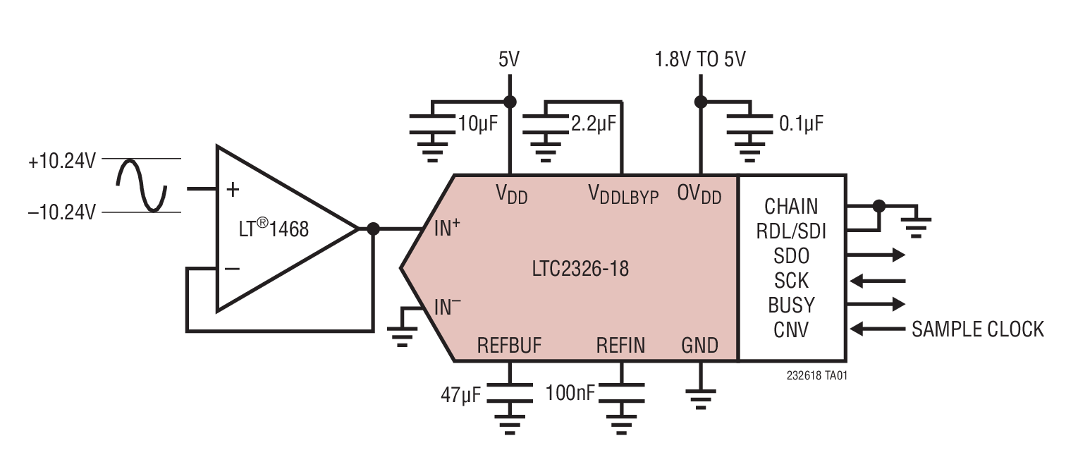
The LTC2326-18 is a low noise, high speed 18-bit successive approximation register (SAR) ADC with pseudo-differential inputs. Operating from a single 5V supply, the LTC2326-18 has a ?10.24V true bipolar input range, making it ideal for high voltage applications which require a wide dynamic range. The LTC2326-18 achieves ?5LSB INL maximum, no missing codes at 18 bits with 95dB SNR.The LTC2326-18 has an onboard single-shot capable reference buffer and low drift (20ppm/?C max) 2.048V temperature compensated reference. The LTC2326-18 also has a high speed SPI-compatible serial interface that supports 1.8V, 2.5V, 3.3V and 5V logic while also featuring a daisy-chain mode. The fast 250ksps throughput with no cycle latency makes the LTC2326-18 ideally suited for a wide variety of high speed applications. An internal oscillator sets the conversion time, easing external timing considerations. The LTC2326-18 dissipates only 28mW and automatically naps between conversions, leading to reduced power dissipation that scales with the sampling rate. A sleep mode is also provided to reduce the power consumption of the LTC2326-18 to 300?W for further power savings during inactive periods. Bits LTC2326-16 16 LTC2326-18 18 Applications Programmable Logic Controllers Industrial Process Control High Speed Data Acquisition Portable or Compact Instrumentation ATE
56-Pin Quad Flatpack No-Lead Logic Package
Texas Instruments
56-Pin Quad Flatpack No-Lead Logic Package
Texas Instruments
Texas Instruments (TI) Quad Flatpack No-Lead (QFN) 56-terminal package complies with JEDEC standard MO-220 allows for board miniaturization and holds several advantages over traditional SOIC TQFP TSSOP and TVSOP packaging. This package designated RGQ by TI physically is smaller than traditional leaded solutions has a smaller routing area improved thermal performance and improved electric
ADIS16477-1/PCBZ

Analog Devices Inc.
ADIS16477-1/PCBZ
Analog Devices Inc.
The ADIS16477 is a precision, miniature MEMS inertial measurement unit (IMU) that includes a triaxial gyroscope and a triaxial accelerometer. Each inertial sensor in the ADIS16477 combines with signal conditioning that optimizes dynamic performance. The factory calibration characterizes each sensor for sensitivity, bias, alignment, linear acceleration (gyroscope bias), and point of percussion (accelerometer location). As a result, each sensor has dynamic compensation formulas that provide accurate sensor measurements over a broad set of conditions.The ADIS16477 provides a simple, cost effective method for integrating accurate, multiaxis inertial sensing into industrial systems, especially when compared with the complexity and investment associated with discrete designs. All necessary motion testing and calibration are part of the production process at the factory, greatly reducing system integration time. Tight orthogonal alignment simplifies inertial frame alignment in navigation systems. The serial peripheral interface (SPI) and register structure provide a simple interface for data collection and configuration control.The ADIS16477 is available in a 44-ball, ball grid array (BGA) package that is approximately 11 mm ? 15 mm ? 11 mm.Applications Navigation, stabilization, and instrumentation Unmanned and autonomous vehicles Smart agriculture/construction machinery Factory/industrial automation, robotics Virtual/augmented reality Internet of Moving Things
Creating Multiple Bit Depth and Multiple Color Pattern Sequences for the DLP? Li (Rev. A)
Texas Instruments
Creating Multiple Bit Depth and Multiple Color Pattern Sequences for the DLP? Li (Rev. A)
Texas Instruments
DLPC300, DLP3000 Creating Multiple Bit Depth and Multiple Color Pattern Sequences for the DLP? Li DLPC300 DLPA035 /DLP/Application_Reports/
LT3645EMSE Demo Board | VIN = 5V to 36V, VOUT1 = 3.3V @ 300mA, VOUT2= 2.5V @ 200mA

Analog Devices Inc.
LT3645EMSE Demo Board | VIN = 5V to 36V, VOUT1 = 3.3V @ 300mA, VOUT2= 2.5V @ 200mA
Analog Devices Inc.
Demonstration circuit 1428A features the dual output LT3645 step-down regulator plus linear regulator. The circuit is designed to convert a 5V to 36V (55V transients) input source to 3.3V at 500mA using the buck regulator and this output is linear regulated down to provide 2.5V at 200mA. Thus the two outputs provide 300mA (buck) and 200mA (LDO).
DC2166A
Analog Devices Inc.
DC2166A
Analog Devices Inc.
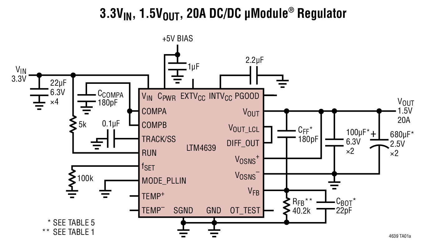
The LTM4639 is a complete 20A output high efficiency switch mode step-down DC/DC ?Module (power module) regulator. Included in the package are the switching controller, power FETs, inductor and compensation components. Operating over an input voltage range from 2.375V to 7V, the LTM4639 supports an output voltage range of 0.6V to 5.5V, set by a single external resistor. Only a few input and output capacitors are needed.Current mode operation allows precision current sharing of up to four LTM4639 regulators to obtain up to 80A output. High switching frequency and a current mode architecture enable a very fast transient response to line and load changes without sacrificing stability. The device supports frequency synchronization, multiphase/current sharing, Burst Mode operation and output voltage tracking for supply rail sequencing. A diode-connected PNP transistor is included for use as an internal temperature monitor. For up to 20V input operation, please see the LTM4637.The LTM4639 is offered in a 15mm ? 15mm ? 4.92mm BGA package. The LTM4639 is RoHS compliant.Applications Telecom Servers and Networking Equipment Industrial Equipment Medical Systems High Ambient Temperature Systems 3.3V Input Systems