
Search results
90VAC-265VAC Input: 12V @ 18W Flyback With Primary-Side Regulation

Texas Instruments
90VAC-265VAC Input: 12V @ 18W Flyback With Primary-Side Regulation
Texas Instruments
The PMP6740 reference design provides 12V at 18W from a universal AC input of 90VAC-265VAC input. This design uses the TL2844 controller with primary side regulation (no optocoupler) for a low cost power solution.
LTC3634EUFD Demo Board (QFN) | VIN= 3.6V to 15V, VOUT1 =1.5V/1.8V/2.5V@±3A, VOUT2 = 0.5VIN (VTT)@±3A, VOUT3 = 0.5VIN (VTTR)@±10mA

Analog Devices Inc.
LTC3634EUFD Demo Board (QFN) | VIN= 3.6V to 15V, VOUT1 =1.5V/1.8V/2.5V@±3A, VOUT2 = 0.5VIN (VTT)@±3A, VOUT3 = 0.5VIN (VTTR)@±10mA
Analog Devices Inc.
Demonstration circuit DC1708A is a dual-output regulator focused specifically for DDR memory power applications. It is built based on the LTC3634, a high voltage dualchannel, controlled on-time monolithic synchronous buck regulator. The DC1708A has an input voltage range of 3.6V to 15V. The output voltage of the first channel, VDDQ, of the DC1708A has three fixed voltage settings: 1.5V, 1.8V and 2.5V, and is capable of delivering up to 3A of output current. The second channel, VTT, is set to regulate to half the voltage on the VDDQIN pin, which can be either the channel 1 output or an external reference voltage. It can source or sink a maximum of 3A of output current. The LTC3634 also provides a 10mA buffered output of half VDDQIN – VTTR, which is used to provide the reference voltage needed for DDR applications. With the use of a timing resistor, the DC1708A can have its operating frequency programmed from 500kHz to 4MHz. Additionally the DC1708A can be easily synchronized to an external clock, due to an internal phase-locked loop, within this same frequency range. The DC1708A VDDQ output can operate in either Burst Mode® operation or forced continuous mode. In Burst Mode operation, which is the preferred mode of low load current operation, the DC supply current is typically only 1.3mA (both channels) at no load (sleep mode), and less than 15µA in shutdown. In Burst Mode operation or continuous mode operation, the DC1708A is a very efficient circuit at high load currents: over 80% for either channel. The LTC3634 is also capable of 90° or 180° out-of-phase operation, and can allow its output to track an external voltage, either coincidentally or ratiometrically. The LTC3634 comes in a 28-pin QFN package, featuring an exposed pad on the bottom-side of the IC for better thermal performance. All of these features make the DC1708A an ideal circuit for powering DDR memory applications.
Class 2- Low Cost 3.3V/1.8A Flyback Converter for PoE Applications

Texas Instruments
Class 2- Low Cost 3.3V/1.8A Flyback Converter for PoE Applications
Texas Instruments
This converter is used for Class 2 or 3 PoE applications. The flyback converter with diode rectifier offers low cost while still achieving good efficiency. This converter is well sutied for PoE applications such as IP phones. The TPS23753A contains both the PoE Powered Device and the PWM controller functions.
Simple Output Filter Eliminates ISO Amp Output Ripple And Keeps Full Bandwidth

Texas Instruments
Simple Output Filter Eliminates ISO Amp Output Ripple And Keeps Full Bandwidth
Texas Instruments
The ISO120/121/122 isolation amplifiers (ISO amps) have a small (10-20mVp-p typ) residual demodulator ripple at the output. A simple filter can be added to eliminate the output ripple without decreasing the 50kHz signal bandwidth of the ISO amp.
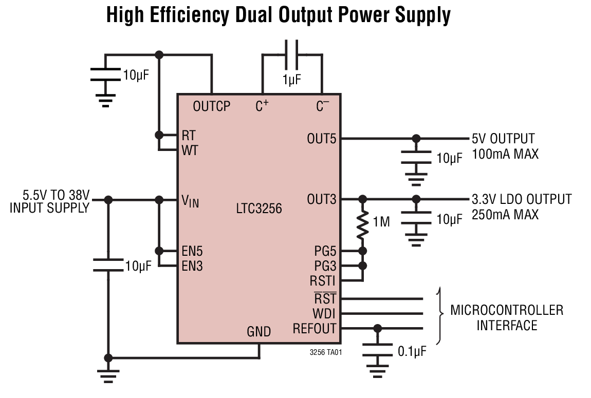
LTC3256 Demo Board | Dual Output Step-Down Charge Pump Plus LDO, 5.5V ≤ VIN ≤ 38V, VOUT1 = 5V @ 100mA, VOUT2 = 3.3V @ 250mA
Analog Devices Inc.
LTC3256 Demo Board | Dual Output Step-Down Charge Pump Plus LDO, 5.5V ≤ VIN ≤ 38V, VOUT1 = 5V @ 100mA, VOUT2 = 3.3V @ 250mA
Analog Devices Inc.
Demonstration Circuit 2375A is a dual output 350mA step down charge pump with a post-regulator LDO and watchdog timer featuring the LTC3256EMSE. The LTC3256 operates with a wide input voltage range from 5.5V to 38V and is engineered for diagnostic coverage in ISO262262 systems. The LTC3256 can provide up to 350mA of output current from a 12V battery with 2W less power dissipation than 2 ideal linear regulators. The DC2375A was populated with automotive grade components for evaluation. Because of the wide input operating range it is possible to exceed the specified operating junction temperature and even reach thermal shutdown with heavy loads. Please refer to the data sheet for additional information on the thermal limitations of the device.
Advanced Profiling with XDS560 Trace (Rev. A)
Texas Instruments
Advanced Profiling with XDS560 Trace (Rev. A)
Texas Instruments
While many developers consider XDS560 Trace a valuable tool for debugging difficult scenarios it also provides quick and effective profiling techniques. With the capability of Trace to capture timestamps on each sample and the flexibility of Advanced Event Triggering to capture data at the appropriate locations XDS560 Trace provides unique profiling capabilities. This application note focuses on
LTC3704EMS Demo Board | 4.5V to 15VIN, –70VOUT1 @ 200mA, –24VOUT2 @ 200mA

Analog Devices Inc.
LTC3704EMS Demo Board | 4.5V to 15VIN, –70VOUT1 @ 200mA, –24VOUT2 @ 200mA
Analog Devices Inc.
Demonstration circuit 518 is a SLIC (Subscriber Line Interface Circuit) positive input to negative output converter featuring the LTC3704 switching controller. DC518 converts 4.5V to 15V input to –24V at 200mA and –70V at 200mA at its output. The demo board uses a transformer with the three primary side widings in parallel to generate three –24V outputs. By stacking the voltages on top of each other, –70V ±10% is obtained. The demo board operates at 200kHz with high efficiency of up to 92%.
Automotive Single-port USB Charging featuring LM43603 and TPS2543 Reference Design

Texas Instruments
Automotive Single-port USB Charging featuring LM43603 and TPS2543 Reference Design
Texas Instruments
Compact design for automotive single-port USB charging featuring the new synchronous 36V: 3A LM43603 SIMPLE SWITCHER and the TPS2543 USB Switch and Controller. LM2904 is used to provide cable droop compensation.
Single-Ended Input to Differential Output Conversion Circuit Reference Design

Texas Instruments
Single-Ended Input to Differential Output Conversion Circuit Reference Design
Texas Instruments
This TI Precision Verified Design provides the theory: component selection: simulation: PCB design: and measurement details for a single ended input to differential output circuit which converts a single ended input of +0.1V to +2.4V into a differential output of ± 2.3V on a single +2.7V supply. The output range is intentionally limited to maximize linearity. The circuit is composed of 2 amplifiers. One amplifier acts as a buffer and creates a voltage: Vout+. The second amplifier inverts the input and adds a reference voltage to generate Vout-. Both Vout+ and Vout- range from 0.1V to 2.4V. The difference: Vdiff: is the difference between Vout+ and Vout-. This makes the differential output voltage range +2.3V.
| Distributor | SKU | Stock | MOQ | 1 | 10 | 50 | 100 | 1,000 | 10,000 | |
|---|---|---|---|---|---|---|---|---|---|---|
| DigiKey | 19-1700/10100-DS-ND | 237 | $1.26 | $0.92 | $0.73 | $0.66 | $0.92 | $0.92 | Buy | |
| Mouser Electronics | 517-1700/10 | 84 | 1 | $66.58 | $62.12 | $50.23 | $45.84 | $45.83 | $45.83 | |
| AVNET Express | 1700/10-100 | 0 | 5 | $50.13 | $46.14 | $44.26 | $44.26 | $44.26 | Buy | |
| Newark | 1700/10-100 | 12 | 1 | $73.66 | $73.66 | $68.43 | $66.18 | $63.94 | $63.94 | Buy |
Interfacing TMS320C5000 DSP to MSP430 Mixed Signal Microcontroller (Rev. A)
Texas Instruments
Interfacing TMS320C5000 DSP to MSP430 Mixed Signal Microcontroller (Rev. A)
Texas Instruments
The TMS320C5000™ family of digital signal processors (DSPs) features Host Port Interface Controllers (HPI) and Direct Memory Access Controllers (DMAC) for efficient data movement without any CPU