
Search results
DC2260A
Analog Devices Inc.
DC2260A
Analog Devices Inc.
The LTC6811 is a multicell battery stack monitor that measures up to 12 series connected battery cells with a total measurement error of less than 1.2mV. The cell measurement range of 0V to 5V makes the LTC6811 suitable for most battery chemistries. All 12 cells can be measured in 290?s, and lower data acquisition rates can be selected for high noise reduction.Multiple LTC6811 devices can be connected in series, permitting simultaneous cell monitoring of long, high voltage battery strings. Each LTC6811 has an isoSPI interface for high speed, RF-immune, long distance communications. Using the LTC6811-1, multiple devices are connected in a daisy chain with one host processor connection for all devices. Using the LTC6811-2, multiple devices are connected in parallel to the host processor, with each device individually addressed.The LTC6811 can be powered directly from the battery stack or from an isolated supply. The LTC6811 includes passive balancing for each cell, with individual PWM duty cycle control for each cell. Other features include an onboard 5V regulator, five general purpose I/O lines and a sleep mode, where current consumption is reduced to 4?A.Applications Electric and Hybrid Electric Vehicles Backup Battery Systems Grid Energy Storage High Power Portable Equipment
LT3085EDCB Demo Board | Single Resistor, Low Dropout Regulator, 1.7V ≤ VIN ≤ 25V, VOUT = 1.2V/1.8V/2.5V/3.3V/5V/Adjustable @ 500mA

Analog Devices Inc.
LT3085EDCB Demo Board | Single Resistor, Low Dropout Regulator, 1.7V ≤ VIN ≤ 25V, VOUT = 1.2V/1.8V/2.5V/3.3V/5V/Adjustable @ 500mA
Analog Devices Inc.
Demonstration circuit 1401A is an adjustable 500mA linear regulator featuring the LT3085. Architected as a precision current source and voltage follower, the LT3085 can be used in many applications requiring up to 500mA output current, adjustability down to 0V at the output and no heat sink. The device brings out the collector of the pass transistor to allow low dropout operation when used with multiple supplies. The demo board operates with an input voltage range from 1.7V to 25V (the maximum output voltage is limited by the output capacitor's voltage rating) and provides a jumper-selectable output voltage of 1.2V, 1.8V, 2.5V, 3.3V, 5V or a user-defined value. For the LT3085 to regulate properly, the voltage on the control pin (VCONTROL) must be more than approximately 1.2V greater than the output voltage.

JESD204B Link Latency Design Using a High Speed ADC

Texas Instruments
JESD204B Link Latency Design Using a High Speed ADC
Texas Instruments
JESD204B links are the latest trend in data-converter digital interfaces. These links take advantage of high-speed serial-digital technology to offer many compelling benefits including improved channel densities. This reference design addresses one of the challenges of adopting the new interface: understanding and designing the link latency. An example achieves deterministic latency and determines the link latency of a system containing the Texas Instruments LM97937 ADC and Xilinx Kintex 7 FPGA.
Single-Ended Input to Differential Output Conversion Circuit Reference Design

Texas Instruments
Single-Ended Input to Differential Output Conversion Circuit Reference Design
Texas Instruments
This TI Precision Verified Design provides the theory: component selection: simulation: PCB design: and measurement details for a single ended input to differential output circuit which converts a single ended input of +0.1V to +2.4V into a differential output of ± 2.3V on a single +2.7V supply. The output range is intentionally limited to maximize linearity. The circuit is composed of 2 amplifiers. One amplifier acts as a buffer and creates a voltage: Vout+. The second amplifier inverts the input and adds a reference voltage to generate Vout-. Both Vout+ and Vout- range from 0.1V to 2.4V. The difference: Vdiff: is the difference between Vout+ and Vout-. This makes the differential output voltage range +2.3V.
TPS6501x Device Comparison (Rev. B)

Texas Instruments
TPS6501x Device Comparison (Rev. B)
Texas Instruments
This application report presents an overview on the differences among the TPS6501x family members. Devices included are the TPS65010, TPS65011, TPS65012,TPS65013, and TPS65014. It is intended to assis
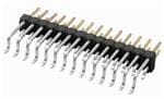
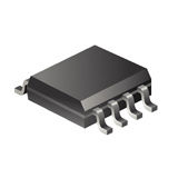
SI3010-F-FS
Silicon Laboratories (Silicon Labs)
From $3.96 • 74 units available from multiple sources
SI3010-F-FS
Silicon Laboratories (Silicon Labs)
Direct Access Arrangement (DAA) 8-Pin SOIC EP
| Distributor | SKU | Stock | MOQ | 1 | 10 | 50 | 100 | 1,000 | 10,000 | |
|---|---|---|---|---|---|---|---|---|---|---|
| DigiKey | 336-4475-1-ND | 54 | 1 | $7.03 | $7.03 | $6.77 | $6.51 | $3.96 | $3.96 | |
| Mouser Electronics | 634-SI3010-FS | 20 | 1 | $7.08 | $6.95 | $6.69 | $6.56 | $5.81 | $5.81 | |
| AVNET Express | SI3010-F-FS | 0 | 48 | $2.86 | $2.85 | $2.83 | $2.83 | Buy | ||
| AVNET Europe | SI3010-F-FS | 0 | 1 | $2.60 | $2.58 | $2.54 | $2.53 | $2.53 | $2.53 | Buy |
| Win Source | SI3010-F-FS | 7,000 | 18 | Buy |
ADP8140EB-EVALZ

Analog Devices Inc.
ADP8140EB-EVALZ
Analog Devices Inc.
The ADP8140 provides high current control of up to four LED drivers. Each driver can sink up to 500 mA. The sink current is programmed for all four drivers with one external resistor.The device features a feedback output that controls an external power supply for optimal efficiency. The ADP8140 also protects the LEDs, power supply, and itself against thermal events, short circuits, overvoltages, and LED open circuits. Multiple ADP8140 ICs are easily connected in parallel to drive additional LED strings or higher current LEDs. The ADP8140 is available in a small, thermally enhanced, lead frame chip scale package (LFCSP).Applications High brightness LED lighting Large format LED backlighting
PTS530GK055SMTRLFS
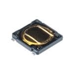
C&K Components
From $0.12 • 1 k+ units available from multiple sources
| Distributor | SKU | Stock | MOQ | 1 | 10 | 50 | 100 | 1,000 | 10,000 | |
|---|---|---|---|---|---|---|---|---|---|---|
| DigiKey | CKN10891CT-ND | 0 | 7,000 | $0.18 | Buy | |||||
| Mouser Electronics | 611-PTS530GK055SMTR | 3,897 | 1 | $0.26 | $0.24 | $0.24 | $0.22 | $0.16 | $0.16 | Buy |
| AVNET Express | PTS530GK055SMTRLFS | 5,781 | 7,000 | $0.22 | Buy | |||||
| TME | PTS530GK055SMTRLFS | 7,000 | Buy | |||||||
| AVNET Europe | PTS530GK055SMTRLFS | 0 | 7,000 | Buy | ||||||
| AVNET Asia Pacific | PTS530GK055SMTRLFS | 0 | 7,000 | Buy | ||||||
| Ameya360 | PTS530GK055SMTRLFS | 0 | $0.15 | Buy | ||||||
| Jak Electronics | PTS530GK055SMTRLFS | 0 | Buy |
LTC6360 Driving LTC2364-16 Demo Board | 16-Bit, 0.25Msps SAR ADC (Requires DC590 or DC718)

Analog Devices Inc.
LTC6360 Driving LTC2364-16 Demo Board | 16-Bit, 0.25Msps SAR ADC (Requires DC590 or DC718)
Analog Devices Inc.
DC1796A-D Demo Board for: LTC6360 Very Low Noise Single-Ended SAR ADC Driver with True Zero Output LTC2364-16 16-Bit, 250ksps, Pseudo-Differential Unipolar SAR ADC with 94.7dB SNR
Low Cost 32V@3A Boost Converter Efficiently Powers Inkjet Printer Reference Design

Texas Instruments
Low Cost 32V@3A Boost Converter Efficiently Powers Inkjet Printer Reference Design
Texas Instruments
This boost converter operates from a 24V supply and regulates a 32V@3A output. The converter is designed with low cost in mind: but also delivers 96% efficiency. Aluminum output caps effectively handle large load current transients.
Pack-Side Impedance Track Fuel Gauge

Texas Instruments
Pack-Side Impedance Track Fuel Gauge
Texas Instruments
The Texas Instruments bq27411-G1 reference design is an easy to configure fuel gauging solution for single series cell Li-Ion battery packs. The device requires minimal configuration and uses One Time Programmable (OTP) Non-Volatile Memory (NVM) to avoid an initialization download by the system processor.The bq27411-G1 uses the patented Impedance Track™ algorithm for fuel gauging: and provides information such as remaining battery capacity (mAh): state-of-charge (%): and battery voltage (mV).
ADP2108-1.5-EVALZ

Analog Devices Inc.
ADP2108-1.5-EVALZ
Analog Devices Inc.
The ADP2108 is a high efficiency, low quiescent current step-down dc-to-dc converter manufactured in two different packages. The total solution requires only three tiny external components. It uses a proprietary, high speed current mode, constant frequency PWM control scheme for excellent stability and transient response. To ensure the longest battery life in portable applications, the ADP2108 has a power save mode that reduces the switching frequency under light load conditions.The ADP2108 runs on input voltages of 2.3 V to 5.5 V, which allows for single lithium or lithium polymer cell, multiple alkaline or NiMH cell, PCMCIA, USB, and other standard power sources. The maximum load current of 600 mA is achievable across the input voltage range.The ADP2108 is available in fixed output voltages of 3.3 V, 3.0 V, 2.5 V, 2.3 V, 1.82 V, 1.8 V, 1.5 V, 1.3 V, 1.2 V, 1.1 V, and 1.0 V. All versions include an internal power switch and synchronous rectifier for minimal external part count and high efficiency. The ADP2108 has an internal soft start and is internally compensated. During logic controlled shutdown, the input is disconnected from the output and the ADP2108 draws less than 1 ?A from the input source.Other key features include undervoltage lockout to prevent deep battery discharge and soft start to prevent input current over-shoot at startup. The ADP2108 is available in 5-ball WLCSP and 5-lead TSOT packages. The ADP2109 provides the same features and operations as the ADP2108 and has the additional function of a discharge switch in the WLCSP package.APPLICATIONS PDAs and palmtop computers Wireless handsets Digital audio, portable media players Digital cameras, GPS navigation units
EVAL-AD5677RSDZ
Analog Devices Inc.
EVAL-AD5677RSDZ
Analog Devices Inc.
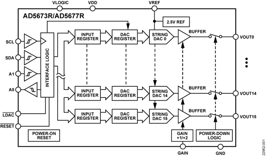
The AD5673R/AD5677R are low power, 16-channel, 12-/16-bit, buffered voltage output, digital-to-analog converters (DACs) that include a 2.5 V, 2 ppm/?C internal reference (enabled by default), and a gain select pin, resulting in a full-scale output of 2.5 V (gain = 1) or 5 V (gain = 2). The devices operate from a single, 2.7 V to 5.5 V supply range and are guaranteed monotonic by design. The AD5673R/AD5677R are available in a 28-lead lead frame chip scale package (LFCSP) and incorporate a power-on reset (POR) circuit that ensures that the DAC outputs power up to and remain at zero scale or midscale until a valid write. The AD5673R/AD5677R contain a power-down mode that reduces the current consumption to 2 ?A typical.Applications Optical transceivers Base station power amplifiers Process control (programmable logic controller (PLC) input/output cards) Industrial automation Data acquisition systems Product Highlights High channel density: 16 channels in 4 mm ? 4 mm LFCSP. High relative accuracy (INL). AD5673R (12-bit): ?1 LSB maximum. AD5677R (16-bit): ?4 LSB maximum. Low drift, 2.5 V, on-chip reference.