
Search results
CC1101-CC1190EM 869 MHz Reference Design

Texas Instruments
CC1101-CC1190EM 869 MHz Reference Design
Texas Instruments
The CC1101-CC1190EM 869MHz reference design contains schematics and layout files for the CC1101-CC1190EM 869MHz evaluation module. The reference design demonstrates good techniques for CC1101-CC1190 decoupling and RF layout. For optimum RF performance: these parts should be copied accurately. This is a 4-layer reference design with a discrete balun and an SMA antenna connector designed for a single ended 50 ohm antenna. The RF section has been designed and characterized for operation in the 869.4 - 869.65 MHz frequency sub-band (g3): but can also be used for other frequencies in the European 863 - 870 MHz band.
EV-ADA4571RSDZ

Analog Devices Inc.
EV-ADA4571RSDZ
Analog Devices Inc.
The ADA4571 is an anisotropic magnetoresistive (AMR) sensorwith integrated signal conditioning amplifiers and ADC drivers.The ADA4571 produces two analog outputs that indicate theangular position of the surrounding magnetic field.The ADA4571 consists of two die within one package, an AMRsensor, and a fixed gain (G = 40 nominally) instrumentationamplifier. The ADA4571 delivers clean and amplified cosineand sine output signals related to the angle of a rotatingmagnetic field. The output voltage range is ratiometric to thesupply voltage.The sensor contains two Wheatstone bridges, at a relative angleof 45? to one another. A rotating magnetic field in the x-ysensor plane delivers two sinusoidal output signals with thedouble frequency of the angle (?) between sensor and magneticfield direction. Within a homogeneous field in the x-y plane,the output signals are independent of the physical placement inthe z direction (air gap).The ADA4571 is available in an 8-lead SOIC package.Product Highlights Contactless angular measurement. Measures magnetic field direction rather than field intensity. Minimum sensitivity to air gap variations. Large working distance. Excellent accuracy, even for weak saturation fields. Minimal thermal and lifetime drift. Negligible hysteresis. Single chip solution.Applications Absolute position measurement (linear and angle) Brushless dc motor control and positioning Actuator control and positioning Contactless angular measurement and detection Magnetic angular position sensing
DC1908A-F
Analog Devices Inc.
DC1908A-F
Analog Devices Inc.
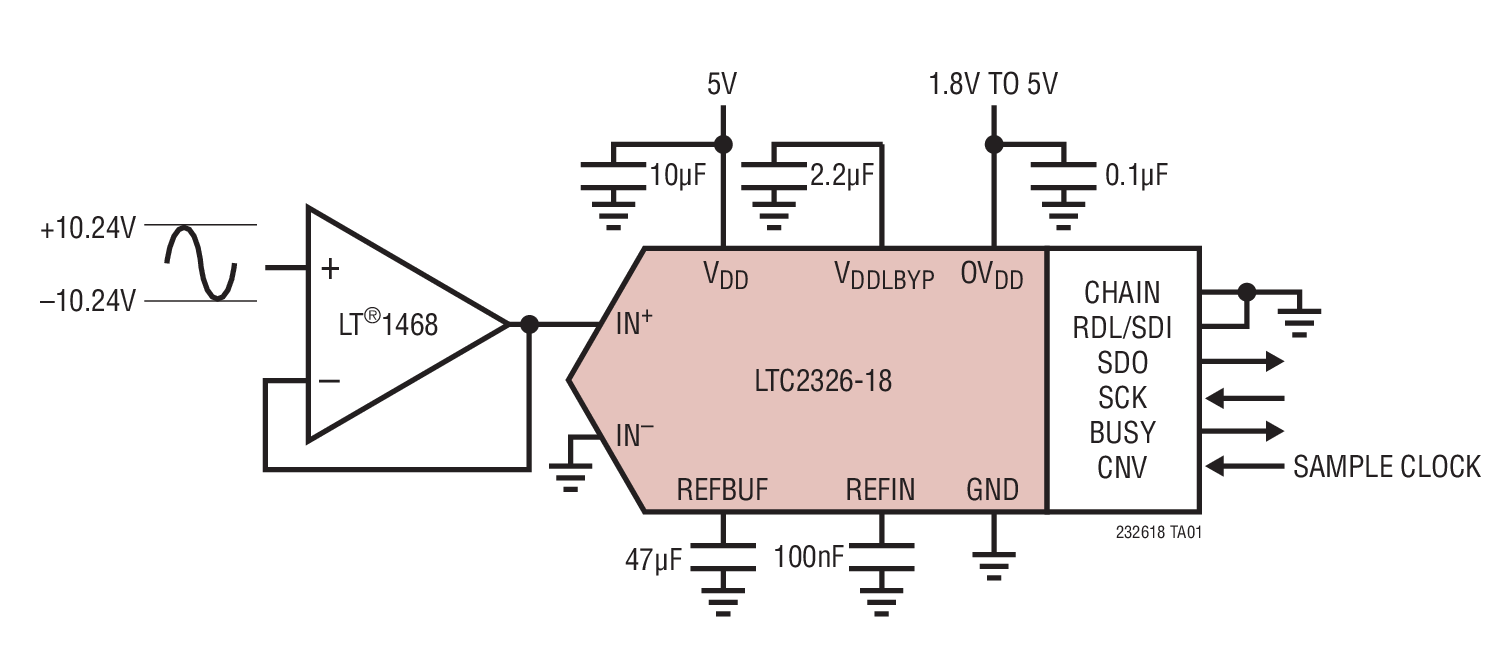
The LTC2326-18 is a low noise, high speed 18-bit successive approximation register (SAR) ADC with pseudo-differential inputs. Operating from a single 5V supply, the LTC2326-18 has a ?10.24V true bipolar input range, making it ideal for high voltage applications which require a wide dynamic range. The LTC2326-18 achieves ?5LSB INL maximum, no missing codes at 18 bits with 95dB SNR.The LTC2326-18 has an onboard single-shot capable reference buffer and low drift (20ppm/?C max) 2.048V temperature compensated reference. The LTC2326-18 also has a high speed SPI-compatible serial interface that supports 1.8V, 2.5V, 3.3V and 5V logic while also featuring a daisy-chain mode. The fast 250ksps throughput with no cycle latency makes the LTC2326-18 ideally suited for a wide variety of high speed applications. An internal oscillator sets the conversion time, easing external timing considerations. The LTC2326-18 dissipates only 28mW and automatically naps between conversions, leading to reduced power dissipation that scales with the sampling rate. A sleep mode is also provided to reduce the power consumption of the LTC2326-18 to 300?W for further power savings during inactive periods. Bits LTC2326-16 16 LTC2326-18 18 Applications Programmable Logic Controllers Industrial Process Control High Speed Data Acquisition Portable or Compact Instrumentation ATE
EVAL-AD7175-2SDZ

Analog Devices Inc.
EVAL-AD7175-2SDZ
Analog Devices Inc.
The AD7175-2 is a low noise, fast settling, multiplexed, 2-/4-channel (fully/pseudo differential) ?-? analog-to-digital converter(ADC) for low bandwidth inputs. It has a maximum channelscan rate of 50 kSPS (20 ?s) for fully settled data. The outputdata rates range from 5 SPS to 250 kSPS.The AD7175-2 integrates key analog and digital signal conditioningblocks to allow users to configure an individual setup foreach analog input channel in use. Each feature can be user selectedon a per channel basis. Integrated true rail-to-rail buffers on theanalog inputs and external reference inputs provide easy to drivehigh impedance inputs. The precision 2.5 V low drift (2 ppm/?C)band gap internal reference (with output reference buffer) addsembedded functionality to reduce external component count.The digital filter allows simultaneous 50 Hz/60 Hz rejection at27.27 SPS output data rate. The user can switch betweendifferent filter options according to the demands of eachchannel in the application. The ADC automatically switchesthrough each selected channel. Further digital processingfunctions include offset and gain calibration registers,configurable on a per channel basis.The device operates with a 5 V AVDD1, or ?2.5 V AVDD1/AVSS,and 2 V to 5 V AVDD2 and IOVDD supplies. The specifiedoperating temperature range is ?40?C to +105?C. The AD7175-2 isin a 24-lead TSSOP package.Applications Process control: PLC/DCS modules Temperature and pressure measurement Medical and scientific multichannel instrumentation Chromatography
Standalone Synchronous Switch-mode Li-Ion Charger with 2A FET Reference Design

Texas Instruments
Standalone Synchronous Switch-mode Li-Ion Charger with 2A FET Reference Design
Texas Instruments
This reference design is a solution for a Li-Ion charge management IC. It has a highly integrated battery charge IC utilizing synchronous switch mode power conversion for efficient and comprehensive charge control of a single cell Li-Ion battery. The solutionprovides a convenient method to evaluate the operation and performance of the IC.
ADP1706-3.3-EVALZ

Analog Devices Inc.
ADP1706-3.3-EVALZ
Analog Devices Inc.
The ADP1706/ADP1707/ADP1708 are CMOS, low dropout linear regulators that operate from 2.5 V to 5.5 V and provide up to 1 A of output current. Using an advanced proprietary architecture, they provide high power supply rejection and achieve excellent line and load transient response with a small 4.7 ?F ceramic output capacitor.The ADP1706/ADP1707 are available in 16 fixed output volt-age options. The ADP1708 is available in an adjustable version, which allows output voltages that range from 0.8 V to 5.0 V via an external divider. The ADP1706 allows an external soft start capacitor to be connected to program the start-up time; the ADP1707 and ADP1708 contain internal soft start capacitors that give a typical start-up time of 100 ?s. The ADP1707 includes a tracking feature that allows the output to follow an external voltage rail or reference.The ADP1706/ADP1707/ADP1708 are available in an 8-lead, exposed paddle SOIC package and an 8-lead, 3 mm ? 3 mm exposed paddle LFCSP, making them not only very compact solutions but also providing excellent thermal performance for applications requiring up to 1 A of output current in a small, low profile footprint. APPLICATIONS Notebook computers Memory components Telecommunications equipment Network equipment DSP/FPGA/microprocessor supplies Instrumentation equipment/data acquisition systems
ADM1270RQ-EVALZ

Analog Devices Inc.
ADM1270RQ-EVALZ
Analog Devices Inc.
The ADM1270 is a current-limiting controller that providesinrush current limiting and overcurrent protection for modularor battery-powered systems. When circuit boards are insertedinto a live backplane, discharged supply bypass capacitors drawlarge transient currents from the backplane power bus as theycharge. These transient currents can cause permanent damageto connector pins, as well as dips on the backplane supply thatcan reset other boards in the system.The ADM1270 is designed to control the inrush current, whenpowering on the system, via an external P-channel field effecttransistor (FET).To protect the system from a reverse polarity input supply, thereis a provision made to control an additional external P-channelFET. This feature prevents reverse current flow in case of a reversepolarity connection, which can damage the load or the ADM1270.The ADM1270 is available in a 3 mm ? 3 mm, 16-lead LFCSP anda 16-lead QSOP. Applications Industrial modules Battery-powered/portable instrumentation
DC2073B-E

Analog Devices Inc.
DC2073B-E
Analog Devices Inc.
The LTC6905-X series of parts are precision, fixed frequency, silicon oscillators designed to minimize board space while maximizing accuracy and ease of use.Programmed at the factory to a fixed frequency, the LTC6905-X series of parts need no external trim components. An internal three-state divider allows for division of the master clock by 1, 2 or 4, providing 3 frequencies (for each device).The LTC6905-X series operate with a single 2.7V to 5.5V power supply and provide a rail-to-rail, 50% duty cycle, square wave output. The OE pin will disable the output when brought low and synchronously enable the output when brought high, avoiding pulse slivers.The four products of the LTC6905-X family are: LTC6905-133: fOSC = 133MHz, 66.7MHz, 33.3MHz LTC6905-100: fOSC = 100MHz, 50MHz, 25MHz LTC6905-96: fOSC = 96MHz, 48MHz, 24MHz LTC6905-80: fOSC = 80MHz, 40MHz, 20MHz?The LTC6905-X series of parts are designed with a factory trim option to modify the divider ratios from 1, 2, 4 to 8, 16, 32. A second trim option allows for additional master clock frequencies. For the alternate divider ratios and unlisted frequencies, contact LTC marketing.Protected by U.S. Patents, including 6614313, 6342817.Applications Data Clocks for High Reliability Applications High Vibration, High Acceleration Environments Replacement for Fixed Crystal and Ceramic Oscillators
Class 4 - Wide Input Range 15W Power over Ethernet (PoE) Converter

Texas Instruments
Class 4 - Wide Input Range 15W Power over Ethernet (PoE) Converter
Texas Instruments
Note: TIDA-00091 was implemented using hardware from PMP6659.The Class 4 – Wide Input Range: 15W Power over Ethernet (PoE) Converter reference design is intended as an evaluation module for users to develop end-products for IP security camera applications. This reference design has been optimized for its wide input voltage range; delivering an output power of 12-V at 1.25-A (15-W) from either an adapter input (10.8 to 57-VDC or 18 to 32-VAC) or power over Ethernet. The wide input voltage range makes this design compatible with legacy applications where 12- or 24-VDC: or 24-VAC auxiliary power is used.
Booting a TMS320C32 Target System in a C Environment
Texas Instruments
Booting a TMS320C32 Target System in a C Environment
Texas Instruments
TI supports four methods of booting a 32-bit floating point DSP following system reset. Each method uses a different combination of the TMS320C32 silicon features software and hardware tools. Each combination forms an integrated development environment that includes features to support most system boot requirements. This document describes in detail the four methods of system boot and provid
LT3480 HV Buck Regulator Board with Plug in Interface

Analog Devices Inc.
LT3480 HV Buck Regulator Board with Plug in Interface
Analog Devices Inc.
Demonstration Circuit 1394A shows how the LT3480 high voltage step-down regulator can be used with the LTC4098 USB-compatible Li-Ion battery charger to design a 2 input source battery charger circuit that also provides power to the load from the LT3480, a 5V wall adapter or the batteries based on available power. The LTC4098 interfaces with a number of ADI switching regulators to provide a high efficiency, high voltage power path. The LT3480 operates from 8V to 38V (60V transients) and provides 2A with a voltage range that is mode and load dependent.
Comparator with Hysteresis Reference Design

Texas Instruments
Comparator with Hysteresis Reference Design
Texas Instruments
This TI Verified Design implements a comparator with hysteresis. Comparators are used to differentiate between two different signal levels. For example: a comparator may differentiate between an over temperature and normal temperature condition. Noise or signal variation at the comparison threshold will cause multiple transitions. Hysteresis sets an upper and lower threshold to eliminate the multiple transitions caused by noise.
LTC3853EUJ Demo Board | Triple, PolyPhase, 6.5V ≤ VIN ≤ 14V, VOUT1 = 1.8V/15A, VOUT2 = 1.2V/15A, VOUT3 = 2.5V/15A

Analog Devices Inc.
LTC3853EUJ Demo Board | Triple, PolyPhase, 6.5V ≤ VIN ≤ 14V, VOUT1 = 1.8V/15A, VOUT2 = 1.2V/15A, VOUT3 = 2.5V/15A
Analog Devices Inc.
Demonstration circuit 1349A is a polyphase 3-output step-down supply with tracking featuring the LTC3853EUJ. The input voltage range is 6.5V to 14V. For applications with narrow, 5V ±0.5V input range, the board has an optional resistor to tie the INTVCC pin to the VIN pin. The demo board provides three 15A outputs, with output voltages of 1.8V, 1.2V and 2.5V. The main features of the board include rail tracking, an internal 5V linear regulator for bias, RUN pins for each output, two PGOOD signals and a Mode selector that allow the converter to run in CCM, pulse skip or Burst Mode operation. Synchronization to an external clock is also possible through some minor component changes.
20W AC/DC PSR isolated LED Driver for T8

Texas Instruments
20W AC/DC PSR isolated LED Driver for T8
Texas Instruments
This reference design demonstrates low cost: high PF LED Driver solution for T8: which includes single stage Flyback with Primary Side Regulation topology using TPS92310. The input range is 85~265Vac and output is 38~42V 420mA or 26~42V 420mA
Implementing SimpleLink Wi-Fi Connectivity in a Smart Electric Meter

Texas Instruments
Implementing SimpleLink Wi-Fi Connectivity in a Smart Electric Meter
Texas Instruments
This design implements a three-phase energy meter with Wi-Fi connectivity. The e-meter SoC is used to perform all metrology functions and control the SimpleLink™ Wi-Fi transceiver. The smart meter data can then be displayed on any Wi-Fi connected device via a standard web browser.
