
Search results
15V – 50V input to 12V@5A: Non Sync Buck

Texas Instruments
15V – 50V input to 12V@5A: Non Sync Buck
Texas Instruments
It is a non synchronous buck controller. It uses a constant on time (COT) device i.e. LM5085.This circuit has ceramic output capacitors which have very low ESR. Therefore the ripple is generated using the DCR of the inductor. The ripple voltage is then superimposed onto the feedback voltage.
AD8376-EVALZ

Analog Devices Inc.
AD8376-EVALZ
Analog Devices Inc.
The AD8376 is a dual channel, digitally controlled, variable gain wide bandwidth amplifier that provides precise gain control, high IP3, and low noise figure. The excellent distortion performance and high signal bandwidth make the AD8376 an excellent gain control device for a variety of receiver applications. Using an advanced high speed SiGe process and incorporating proprietary distortion cancellation techniques, the AD8376 achieves 50 dBm output IP3 at 200 MHz. The AD8376 provides a broad 24 dB gain range with 1 dB resolution. The gain of each channel is adjusted through dedicated 5-pin control interfaces and can be driven using standard TTL levels. The open-collector outputs provide a flexible interface, allowing the overall signal gain to be set by the loading impedance. Thus, the signal voltage gain is directly proportional to the load. Each channel of the AD8376 can be individually powered on by applying the appropriate logic level to the ENBA and ENBB power enable pins. The quiescent current of the AD8376 is typically 130 mA per channel. When powered down, the AD8376 consumes less than 5 mA and offers excellent input-to-output isolation, lower than ?50 dB at 200 MHz. Fabricated on an Analog Devices, Inc., high speed SiGe process, the AD8376 is supplied in a compact, thermally enhanced, 5 mm ? 5mm 32-lead LFCSP package and operates over the temperature range of ?40?C to +85?C.ApplicationsDifferential ADC drivers Main and diversity IF sampling receivers Wideband multichannel receivers Instrumentation Data Sheet, Rev. 0, 8/07
DC/DC Sync Buck Converter 48Vin to 8-30Vout 12A Reference Design
Texas Instruments
DC/DC Sync Buck Converter 48Vin to 8-30Vout 12A Reference Design
Texas Instruments
The TPS40170 controller with a pair 60V FETs from our CSD1835x offerings provide a complete high efficiency solution for non-isolated DC/DC needs off a regulated 48V input voltage. The attached design targeted 30V output at 12A and achieved 98% conversion efficiency. The same design was then adjusted to 8V output at same current and test results for this are also attached. The attached Test Reports include thermal images both with and without forced airflow. For lower current applications or applications with significant airflow; lower cost FETs from the CSD1835x series can be used. For outputs at 12Vouts or less: even at same 12A current; a smaller output choke can be used.
180W RGB LED Drivers for DLP Projector application
Texas Instruments
180W RGB LED Drivers for DLP Projector application
Texas Instruments
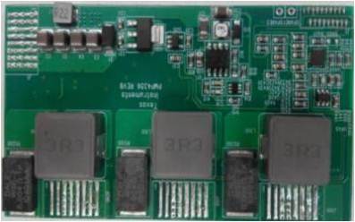
The PMP4356 is RGB LED drivers solution which used in high power density DLP projector. LM3434 and power block CSD87350 are used in each rail to provide up to 15A of drive ability. The design demostrates high efficiency up to 92.5%@full load within the form factor of 80mm*45mm*10.8mm with good dimming performance.
LT8644S | 8V, 16A Synchronous Step-Down Silent Switcher 2

Analog Devices Inc.
LT8644S | 8V, 16A Synchronous Step-Down Silent Switcher 2
Analog Devices Inc.
Demonstration circuit 2779A is an 8V, 16A synchronous step-down Silent Switcher® 2 with spread spectrum frequency modulation featuring the LT8644S. The demo board is designed for 1.2V output from a 2.7V to 8V input. The LT8644S is a compact, ultralow emission, high efficiency, and high speed synchronous monolithic stepdown switching regulator. The integrated bypass capacitors optimize all the fast current loops and make it easier to minimize EMI emissions by reducing layout sensitivity. Selectable spread spectrum mode further improves EMI performance, making it perfect solution to the noise sensitive applications. Peak current mode control with minimum on-time of as low as 20ns allows high step-down conversion even at high frequency. The LT8644S switching frequency can be programmed either via an external resistor or an external clock over a 300kHz to 3.5MHz range. The default frequency of demo circuit 2779A is 2MHz. The SYNC/MODE pin on the demo board DC2779A is grounded (JP1 at BURST position) by default for low ripple Burst Mode® operation. It can be configured into different operation modes through JP1 and SYNC terminal (Table 1 in the demo manual). Figure 4 in the demo manual shows the efficiency of the circuit at 3.3V input and 5V input in force continuous mode operation (input from VIN terminal). To get accurate efficiency measurement, measure the input voltage at the VIN_SENSE/GND terminals and measure the output voltage at the VOUT+ SENSE/VOUT– SENSE terminals. Figure 5 shows the LT8644S temperature rise on DC2779A demo board at 3.3V input and 5V input in forced continuous mode. The LT8644S is assembled in a 4mm × 4mm LQFN package with exposed pads for low thermal resistance. The rated maximum continuous load current is 16A, while derating may be necessary for certain input voltage and thermal conditions. The demo board has an EMI filter installed. This EMI filter can be included by applying the input voltage at the VEMI terminal. The EMI performance of the board (with EMI filter) is shown on Figure 6 in the demo manual. The red lines in EMI Performance are CISPR25 Class 5 limits. The figure shows that the LT8644S circuit passes the test with a wide margin. To achieve EMI performance as shown in Figure 6, the input EMI filter is required and the input voltage should be applied to VEMI terminal, and the test setup can be referred to the CISPR25 standards. If the input is applied to VIN terminal, the EMI filter is bypassed. The LT8644S data sheet gives a complete description of the part, the operation and application information. The data sheet must be read in conjunction with the demo manual for demo circuit 2779A. The layout recommendations for low EMI operation and maximum thermal performance are available in the data sheet section Low EMI PCB Layout and Thermal Considerations. Contact ADI applications engineer for support.


1/8 Brick Isolated DC/DC Telecom Power Module Digital Control Reference Design

Texas Instruments
1/8 Brick Isolated DC/DC Telecom Power Module Digital Control Reference Design
Texas Instruments
PMP8877 is a full-function 1/8th brick isolated DC/DC telecom power module based on the UCD3138 digital power controller. The reference design features secondary side control and hard switching full bridge power topology to deliver 12V/180W of output power operating across a wide range 36V-72V input source. The highlights of the reference design include 94% peak efficiency: fast input voltage feedforward response to input voltage surges: constant current/constant power overload protection: pre-bias start-up: current sharing control for paralleled module applications and PMBUS support for communication with peer controllers. The bias supply block employs the UCC25230: while the gate drivers used in this design include UCC27524 for driving the SR MOSFETs and UCC27211 for driving the primary side Half-Bridge MOSFETs. Other components include the ISO7240 for sending signals across the isolation barrier.
EVAL-AD1937AZ

Analog Devices Inc.
EVAL-AD1937AZ
Analog Devices Inc.
The AD1937 is a high performance, single-chip codec that provides four analog-to-digital converters (ADCs) with differential input and eight digital-to-analog converters (DACs) with differential output, using the Analog Devices, Inc., patented multibit sigma-delta (?-?) architecture. An I2C? port is included, allowing a microcontroller to adjust volume and many other parameters. The AD1937 operates from 3.3 V digital and analog supplies. The AD1937 is available in a 64-lead (differential output) LQFP.The AD1937 is designed for low EMI. This consideration is apparent in both the system and circuit design architectures. By using the on-board PLL to derive the master clock from the LR (frame) clock or from an external crystal, the AD1937 eliminates the need for a separate high frequency master clock and can also be used with a suppressed bit clock. The DACs and ADCs are designed using the latest Analog Devices continuous time architecture to further minimize EMI. By using 3.3 V supplies, power consumption is minimized and further reduces emissions.ApplicationsAutomotive audio systems Home theater systemsSet-top boxesDigital audio effects processorsData Sheet, Rev. 0, 9/08
CC2420DB Reference Design
Texas Instruments
CC2420DB Reference Design
Texas Instruments
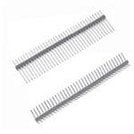
The CC2420DB reference design contains schematics and layout files for the CC2420DB module used in development kits. The reference design demonstrates good techniques for CC2420 decoupling and RF layout. For optimum RF performance: the reference design should be copied accurately. This is a 4-layer reference design with a discrete balun and an inverted F PCB antenna. In addition to the RF part: this design contains a DB-9 serial port and a number of IO units. Most of the CC2420 application examples are using this HW platform.
90 to 290VAC Vin 32W Non-isolated Quasi-Resonant Flyback Reference Design
Texas Instruments
90 to 290VAC Vin 32W Non-isolated Quasi-Resonant Flyback Reference Design
Texas Instruments
The PMP8697 reference design uses the UCC28610 quasi-resonant flyback controller to generate two non-isolated outputs (12V@1.89A: 15V@0.2A) and one isolated output (15V@0.39A).
LMZ12010 20VIN 10AOUT Simple Switcher? Module Reference Design

Texas Instruments
LMZ12010 20VIN 10AOUT Simple Switcher? Module Reference Design
Texas Instruments
The LMZ13610/8 and LMZ12010/8 SIMPLE SWITCHER® power modules are easy-to-use DC-DC solution capable of driving up to a 10A load. They are available in an innovative package that enhances thermal performance and allows for hand or machine soldering. The LMZ13610/8 can accept an input voltage rail between 6V and 36V and the LMZ12010/8 can accept an input voltage rail between 6V and 20V. The devices can deliver an adjustable and highly accurate output voltage as low as 0.8V and as high as 6V. The control structure is constant frequency PWM. The control loop operates well with low ESR output capacitors such as ceramics. The precision enable input allows for programmable UVLO of the input supply. The external soft-start capacitor facilitates a controlled and adjustable startup rise time of the output. The LMZ13610 and LMZ12010 family is a reliable and robust solution with the following features: loss-less cycle-by-cycle valley current limit to protect for over current or short-circuit fault, thermal shutdown, input under-voltage lockout, and will start up into a pre-biased output. Free-running switching frequency is 350 kHz.
ADRF5026-EVALZ-292

Analog Devices Inc.
ADRF5026-EVALZ-292
Analog Devices Inc.
The ADRF5026 is a nonreflective, single-pole, double-throw (SPDT) radio frequency (RF) switch manufactured in a silicon process.The ADRF5026 operates from 100 MHz to 44 GHz with better than 3.8 dB of insertion loss and 45 dB of isolation. The ADRF5026 features an all off control, where both RF ports are in an isolation state. The ADRF5026 has a nonreflective design and both of the RF ports are internally terminated to 50 ?. The ADRF5026 requires a dual-supply voltage of +3.3 V and ?3.3 V. The device employs complimentary metal-oxide semiconductor/low-voltage transistor-transistor logic (CMOS/LVTTL) logic-compatible controls.The ADRF5026 is pin-compatible with the ADRF5027 low frequency cutoff version, which operates from 9 kHz to 44 GHz. The ADRF5026 RF ports are designed to match a characteristic impedance of 50 ?. For ultrawideband products, impedance matching on the RF transmission lines can further optimize high frequency insertion loss and return loss characteristics. Refer to the Narrow-Band Impedance Matching section for an example of a matched circuit that achieves a flat insertion loss response of 2.4 dB from 28 GHz to 43 GHz.The ADRF5026 comes in a 20-terminal, 3 mm ? 3 mm, RoHS-compliant, land grid array (LGA) package and can operate from ?40?C to +105?C.The ADRF5026 supports defense and aerospace applications (AQEC).Applications Industrial scanners Test and instrumentation Cellular infrastructure: 5G mmWave Military radios, radars, electronic counter measures (ECMs) Microwave radios and very small aperture terminals (VSATs)
PTS530GK055SMTRLFS
C&K Components
From $0.12 • 1 k+ units available from multiple sources
| Distributor | SKU | Stock | MOQ | 1 | 10 | 50 | 100 | 1,000 | 10,000 | |
|---|---|---|---|---|---|---|---|---|---|---|
| DigiKey | CKN10891CT-ND | 0 | 7,000 | $0.18 | Buy | |||||
| Mouser Electronics | 611-PTS530GK055SMTR | 3,897 | 1 | $0.26 | $0.24 | $0.24 | $0.22 | $0.16 | $0.16 | Buy |
| AVNET Express | PTS530GK055SMTRLFS | 5,781 | 7,000 | $0.22 | Buy | |||||
| TME | PTS530GK055SMTRLFS | 7,000 | Buy | |||||||
| AVNET Europe | PTS530GK055SMTRLFS | 0 | 7,000 | Buy | ||||||
| AVNET Asia Pacific | PTS530GK055SMTRLFS | 0 | 7,000 | Buy | ||||||
| Ameya360 | PTS530GK055SMTRLFS | 0 | $0.15 | Buy | ||||||
| Jak Electronics | PTS530GK055SMTRLFS | 0 | Buy |
DC2387A

Analog Devices Inc.
DC2387A
Analog Devices Inc.
The LTM8071 is a 60VIN, 5A (continuous) step-down Silent Switcher ?Module? (power module) regulator. The Silent Switcher architecture minimizes EMI while delivering high efficiency at frequencies up to 2.2MHz. Included in the package are the switching controller, power switches, inductor, and all support components. Operating over an input voltage range of 3.6V to 60V, the LTM8071 supports an output voltage range of 0.97V to 15V and a switching frequency range of 200kHz to 2.2MHz, each set by a single resistor. Only the input and output filter capacitors are needed to finish the design.The LTM8071 is packaged in a compact over-molded ball grid array (BGA) package suitable for automated assembly by standard surface mount equipment. The LTM8071 is available with SnPb (BGA) or RoHS compliant terminal finish.APPLICATIONS Test and Measurement Equipment Aviation Distributed Supply Regulation Industrial Supplies Wall Transformer Regulation
Advanced Profiling with XDS560 Trace (Rev. A)
Texas Instruments
Advanced Profiling with XDS560 Trace (Rev. A)
Texas Instruments
While many developers consider XDS560 Trace a valuable tool for debugging difficult scenarios it also provides quick and effective profiling techniques. With the capability of Trace to capture timestamps on each sample and the flexibility of Advanced Event Triggering to capture data at the appropriate locations XDS560 Trace provides unique profiling capabilities. This application note focuses on
Creating Multiple Bit Depth and Multiple Color Pattern Sequences for the DLP? Li (Rev. A)
Texas Instruments
Creating Multiple Bit Depth and Multiple Color Pattern Sequences for the DLP? Li (Rev. A)
Texas Instruments
DLPC300, DLP3000 Creating Multiple Bit Depth and Multiple Color Pattern Sequences for the DLP? Li DLPC300 DLPA035 /DLP/Application_Reports/