
Search results
Qi (WPC) Compliant Wireless Charger for Low Power Wearable Applications

Texas Instruments
Qi (WPC) Compliant Wireless Charger for Low Power Wearable Applications
Texas Instruments
TI design TIDA-00318 is suitable for low power wearable device including a Qi compliant wireless receiver (bq51003)and ultra low current 1 cell Li-ion linear charger (bq25100). It features an ultra small size (5x15mm2), capable of low charging currents down to 10mA and up to 250mAwith support of termination currents as low as 1mA. Current design is designed for 135mA charge current application.
LT3645EMSE Demo Board | VIN = 5V to 36V, VOUT1 = 3.3V @ 300mA, VOUT2= 2.5V @ 200mA

Analog Devices Inc.
LT3645EMSE Demo Board | VIN = 5V to 36V, VOUT1 = 3.3V @ 300mA, VOUT2= 2.5V @ 200mA
Analog Devices Inc.
Demonstration circuit 1428A features the dual output LT3645 step-down regulator plus linear regulator. The circuit is designed to convert a 5V to 36V (55V transients) input source to 3.3V at 500mA using the buck regulator and this output is linear regulated down to provide 2.5V at 200mA. Thus the two outputs provide 300mA (buck) and 200mA (LDO).
AD9228-65KITZ
Analog Devices Inc.
AD9228-65KITZ
Analog Devices Inc.
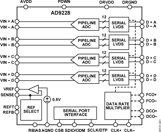
The AD9228 is a quad, 12-bit, 40/65 MSPS analog-to-digital converter (ADC) with an on-chip sample-and-hold circuit designed for low cost, low power, small size, and ease of use. The product operates at a conversion rate of up to 65 MSPS and is optimized for outstanding dynamic performance and low power in applications where a small package size is critical. The ADC requires a single 1.8 V power supply and LVPECL-/ CMOS-/LVDS-compatible sample rate clock for full performance operation. No external reference or driver components are required for many applications. The ADC automatically multiplies the sample rate clock for the appropriate LVDS serial data rate. A data clock output (DCO) for capturing data on the output and a frame clock output (FCO) for signaling a new output byte are provided. Individual channel power-down is supported and typically consumes The ADC contains several features designed to maximize flexibility and minimize system cost, such as programmable clock and data alignment and programmable digital test pattern generation. The available digital test patterns include built-in deterministic and pseudorandom patterns, along with custom user-defined test patterns entered via the serial port interface (SPI). The AD9228 is available in an RoHS compliant, 48-lead LFCSP. It is specified over the industrial temperature range of ?40?C to +85?C.PRODUCT HIGHLIGHTSSmall Footprint. Four ADCs are contained in a small, space-saving package. Low power of 119 mW/channel at 65 MSPS. Ease of Use. A data clock output (DCO) is provided that operates at frequencies of up to 390 MHz and supports double data rate (DDR) operation.User Flexibility. The SPI control offers a wide range of flexible features to meet specific system requirements. Pin-Compatible Family. This includes the AD9287 (8-bit), AD9219 (10-bit), and AD9259 (14-bit).?APPLICATIONSMedical imaging and nondestructive ultrasound Portable ultrasound and digital beam-forming systemsQuadrature radio receivers Diversity radio receivers Tape drives Optical networking Test equipment
Class 3 Multi-Output Flyback Converter for PoE PD Application Reference Design

Texas Instruments
Class 3 Multi-Output Flyback Converter for PoE PD Application Reference Design
Texas Instruments
PMP841 is a high efficiency, non-isolated Power-over-Ethernet PD power supply reference design intended to ease implementation of PoE in devices such as IP phones, WLAN AP's and security cameras. The reference design uses a TPS2375 PoE Powered Device Controller to implement all necessary detection,
EVAL-AD5940ELCZ

Analog Devices Inc.
EVAL-AD5940ELCZ
Analog Devices Inc.
The AD5940 and AD5941 are high precision, low power analog front ends (AFEs) designed for portable applications that require high precision, electrochemical-based measurement techniques, such as amperometric, voltammetric, or impedance measurements. The AD5940/AD5941 is designed for skin impedance and body impedance measurements, and works with the AD8233 AFE in a complete bioelectric or biopotential measurement system. The AD5940/AD5941 is designed for electrochemical toxic gas sensing.The AD5940/AD5941 consist of two high precision excitation loops and one common measurement channel, which enables a wide capability of measurements of the sensor under test. The first excitation loop consists of an ultra low power, dual-output string, digital-to-analog converter (DAC), and a low power, low noise potentiostat. One output of the DAC controls the noninverting input of the potentiostat, and the other output controls the noninverting input of the transimpedance amplifier (TIA). This low power excitation loop is capable of generating signals from dc to 200 Hz.The second excitation loop consists of a 12-bit DAC, referred to as the high speed DAC. This DAC is capable of generating high frequency excitation signals up to 200 kHz.The AD5940/AD5941 measurement channel features a 16-bit, 800 kSPS, multichannel successive approximation register (SAR) analog-to-digital converter (ADC) with input buffers, a built in antialias filter, and a programmable gain amplifier (PGA). An input multiplexer (mux) in front of the ADC allows the user to select an input channel for measurement. These input channels include multiple external current inputs, external voltage inputs, and internal channels. The internal channels allow diagnostic measurements of the internal supply voltages, die temperature, and reference voltages.The current inputs include two TIAs with programmable gain and load resistors for measuring different sensor types. The first TIA, referred to as the low power TIA, measures low bandwidth signals. The second TIA, referred to as the high speed TIA, measures high bandwidth signals up to 200 kHz.An ultra low leakage, programmable switch matrix connects the sensor to the internal analog excitation and measurement blocks. This matrix provides an interface for connecting external transimpedance amplifier resistors (RTIAs) and calibration resistors. The matrix can also be used to multiplex multiple electronic measurement devices to the same wearable electrodes.A precision 1.82 V and 2.5 V on-chip reference source is available. The internal ADC and DAC circuits use this on-chip reference source to ensure low drift performance for the 1.82 V and 2.5 V peripherals.The AD5940/AD5941 measurement blocks can be controlled via direct register writes through the serial peripheral interface (SPI) interface, or, alternatively, by using a preprogrammable sequencer, which provides autonomous control of the AFE chip. 6 kB of static random access memory (SRAM) is partitioned for a deep data first in, first out (FIFO) and command FIFO. Measurement commands are stored in the command FIFO and measurement results are stored in the data FIFO. A number of FIFO related interrupts are available to indicate when the FIFO is full.A number of general-purpose inputs/outputs (GPIOs) are available and controlled using the AFE sequencer. The AFE sequencer allows cycle accurate control of multiple external sensor devices.The AD5940/AD5941 operate from a 2.8 V to 3.6 V supply and are specified over a temperature range of ?40?C to +85?C. The AD5940 is packaged in a 56-lead, 3.6 mm ? 4.2 mm WLCSP. The AD5941 is packaged in a 48-lead LFCSP.APPLICATIONS Electrochemical measurements Electrochemical gas sensors Potentiostat/amperometric/voltammetry/cyclic voltammetry Bioimpedance applications Skin impedance Body impedance Continuous glucose monitoring Battery impedance
TPS40304 Step-Down Regulator Delivering 3.3V at 16A Reference Design
Texas Instruments
TPS40304 Step-Down Regulator Delivering 3.3V at 16A Reference Design
Texas Instruments
PMP4713 is a single-phase synchronous switching regulator accepting an input voltage range of 7.0Vin to 14.0Vin and providing an output voltage of 3.3Vout capable of supplying 16A of current.
180W RGB LED Drivers for DLP Projector application
Texas Instruments
180W RGB LED Drivers for DLP Projector application
Texas Instruments
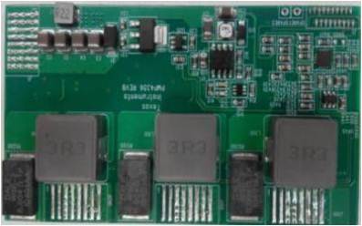
The PMP4356 is RGB LED drivers solution which used in high power density DLP projector. LM3434 and power block CSD87350 are used in each rail to provide up to 15A of drive ability. The design demostrates high efficiency up to 92.5%@full load within the form factor of 80mm*45mm*10.8mm with good dimming performance.
ADL5902-EVALZ

Analog Devices Inc.
ADL5902-EVALZ
Analog Devices Inc.
The ADL5902 is a true rms responding power detector that hasa 65 dB measurement range when driven with a single-ended 50 ? source. This feature makes the ADL5902 frequencyversatile by eliminating the need for a balun or any other form of external input tuning for operation up to 9 GHz.The ADL5902 provides a solution in a variety of high frequencysystems requiring an accurate measurement of signal power. Requiring only a single supply of 5 V and a few capacitors, it is easy to use and capable of being driven single-ended or with abalun for differential input drive. The ADL5902 can operate from 50 MHz to 9 GHz and can accept inputs from ?62 dBm to at least +3 dBm with large crest factors, such as GSM, CDMA,W-CDMA, TD-SCDMA, WiMAX, and LTE modulated signals.The ADL5902 can determine the true power of a high frequency signal having a complex low frequency modulation envelope or can be used as a simple low frequency rmsvoltmeter. Used as a power measurement device, VOUT isconnected to VSET. The output is then proportional to thelogarithm of the rms value of the input. In other words, thereading is presented directly in decibels and is scaled 1.06 V per decade, or 53 mV/dB; other slopes are easily arranged. In controller mode, the voltage applied to VSET determines thepower level required at the input to null the deviation from the set point. The output buffer can provide high load currents.The ADL5902 has 1.5 mW power consumption when powereddown by a logic high applied to the PWDN pin. It powers up within approximately 5 ?s to its nominal operating current of 73 mA at 25?C. The ADL5902 is supplied in a 4 mm ? 4 mm,16-lead LFCSP for operation over the wide temperature rangeof ?40?C to +125?C.The ADL5902 is also pin-compatible with the AD8363, 50 dBdynamic range TruPwr? detector. This feature allows the designer to create one circuit layout for projects requiring different dynamic ranges. A fully populated RoHS-compliant evaluation board is available.Applications Power amplifier linearization/control loops Transmitter power controls Transmitter signal strength indication (TSSI) RF instrumentation
18V-60V Input: 12V@10A Active Clamp Forward

Texas Instruments
18V-60V Input: 12V@10A Active Clamp Forward
Texas Instruments
This reference design provides 12V at 10A from a wide range 18V-60V telecom input with greater than 93% efficiency. This design uses the UCC2897A active clamp controller with synchronous rectifiers for an efficient: yet cost effective solution that can operate from either a 24VDC or 48VDC input bus.
| Distributor | SKU | Stock | MOQ | 1 | 10 | 50 | 100 | 1,000 | 10,000 | |
|---|---|---|---|---|---|---|---|---|---|---|
| DigiKey | 40661-00000-10-ND | 0 | $30.86 | $30.86 | $30.86 | $30.86 | $30.86 | $30.86 | Buy | |
| AVNET Express | 40661-00000-10 | 0 | 1 | $50.07 | $48.37 | $45.22 | $43.82 | $43.82 | $43.82 | Buy |
| Newark | 40661-00000-10 | 1 | 1 | $53.00 | $53.00 | $53.00 | $53.00 | $53.00 | $53.00 | Buy |
| Heiland | MMM7000002378 | 0 | $70.67 | $58.71 | $55.30 | $55.30 | $53.00 | $53.00 | Buy |
Using the Scaler in the TVP5154
Texas Instruments
Using the Scaler in the TVP5154
Texas Instruments
The TVP5154 video decoder product includes the additional functionality of an integrated polymorphic down-scaler for both vertical and horizontal scaling. The video images can be downscaled in both horizontal and vertical directions to an arbitrary size. This Application Note outlines how to correctly use this scaler feature for standard NTSC and PAL video. Also included are the register settings

Integrated Gate Driver for Residential Inverters Reference Design

Texas Instruments
Integrated Gate Driver for Residential Inverters Reference Design
Texas Instruments
The PMP9455 reference design provides a highly integrated gate driver solution for 800VA to 3kVA iPure Sine Wave Low Frequency Inverter application . With its unique features of higher peak current drive capability along with integration of two transconductance amplifier with external programmable gain and filtering : the design is a perfect fit for industrial applications . The daughter card design of SM72295 can also be used in various other four switch power topologies such as Buck Boost: Interleaved Buck etc. The Reference design has also been successfully tested on Solar MPPT charger : the details of which can also be found in TIDA-00120 design (http://www.ti.com/tool/TIDA-00120).
Implementing SimpleLink Wi-Fi Connectivity in a Smart Electric Meter

Texas Instruments
Implementing SimpleLink Wi-Fi Connectivity in a Smart Electric Meter
Texas Instruments
This design implements a three-phase energy meter with Wi-Fi connectivity. The e-meter SoC is used to perform all metrology functions and control the SimpleLink™ Wi-Fi transceiver. The smart meter data can then be displayed on any Wi-Fi connected device via a standard web browser.
What is a .tmap File? (Rev. A)
Texas Instruments
What is a .tmap File? (Rev. A)
Texas Instruments
The PowerLAN™ Master Gateway Battery Management Controller uses a file identified by the .tmap file extension to load configuration parameters. This file serves to configure the operation of the controller to the specific application. Examples of configurable parameters are number of parallel and series cells in the pack number of temperature sensors and state-of-charge indication (SOCi) dis