
Search results for: tps63


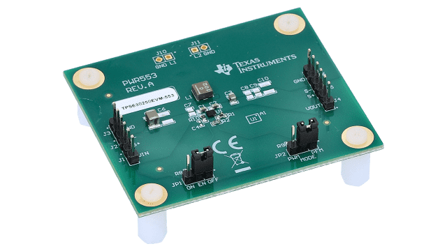


TPS63060EVM-619 Efficient; 2.25A Switch Current Limit; Buck-Boost Converter Evaluation Module

Texas Instruments
TPS63060EVM-619 Efficient; 2.25A Switch Current Limit; Buck-Boost Converter Evaluation Module
Texas Instruments
TPS63060EVM-619 Efficient; 2.25A Switch Current Limit; Buck-Boost Converter Evaluation Module


131384-HMC1010LP4E

Analog Devices Inc.
131384-HMC1010LP4E
Analog Devices Inc.
The HMC1010LP4E Power Detector is designed for RF power measurement, and control applications for frequencies up to 3.9 GHz. The detector provides an accurate RMS representation of any RF/IF input signal. The output is a temperature compensated monotonic, representation of real signal power, measured with an input sensing range of 60 dB.The HMC1010LP4E is ideally suited to those wide bandwidth, wide dynamic range applications, requiring repeatable measurement of real signal power, especially where RF/IF wave shape and/or crest factor change with time.The integration bandwidth of the HMC1010LP4E is digitally programmable with the use of input pins SC I1- 4 with a range of more than 4 decades. This allows the user to dynamically set the operation bandwidth providing the capability of handling different types of modulations on the same platform.The HMC1010LP4E features an internal op-amp at output stage, which provides for slope & intercept adjustments and enables controller application.Applications Log ?> Root-Mean-Square?(RMS) Conversion Received Signal Strength?Indication (RSSI) Transmitter Signal Strength?Indication (TSSI) RF Power Amplifier Efficiency Control Receiver Automatic Gain Control Transmitter Power Control
AD8113-EVALZ

Analog Devices Inc.
AD8113-EVALZ
Analog Devices Inc.
The AD8113 is a fully buffered crosspoint switch matrix that operates on ?12V for Audio applications and ?5V for Video applications. It offers a -3dB signal bandwidth greater than 60MHz and channel switch times of less than 60ns with 0.1% settling for use in both analog and digital audio. The AD8113 operated at 20kHz has crosstalk performance of -83dB and isolation of 90dB. In addition, ground/power pins surround all inputs and outputs to provide extra shielding for operation in the most demanding audio routing applications. The differential gain and differential phase of better than 0.1% and 0.1?, respectively, along with 0.1dB flatness out to 10MHz make the AD8113 suitable for many video applications.The AD8113 includes 16 independent output buffers that can be placed into a disabled state for paralleling crosspoint outputs so that off channel loading is minimized. The AD8113 has a gain of +2. It operates on voltage supplies of ?5V or ?12V while consuming only 34mA or 31mA of current, respectively.The channel switching is performed via a serial digital control (which can accommodate daisy-chaining of several devices) or via a parallel control, allowing updating of an individual output without reprogramming the entire array.The AD8113 is packaged in a 100-lead LQFP and is available over the commercial temperature range of 0?C to 70?C.
AD8334-EVALZ

Analog Devices Inc.
AD8334-EVALZ
Analog Devices Inc.
The AD8334 is an ultralow noise, quad channel linear-in-dB variable gain amplifier (VGA). Although optimized for ultrasound systems, it may be used as a low noise variable gain control in any application whose operating frequency is less than 100 MHz.Included in each channel are an ultralow noise preamp (LNA), an X-AMP? VGA with 48 dB of gain range, and a selectable gain postamp with adjustable output limiting. The LNA gain is 19 dB with a single-ended input and differential outputs. Using a single resistor, the LNA input impedance can be adjusted to match a signal source without compromising noise performance.The 48 dB gain range of the VGA makes these devices suitable for a variety of applications. Excellent bandwidth uniformity is maintained across the entire range. The gain control interface provides precise linear-in-dB scaling of 50 dB/V for control voltages between 40 mV and 1 V. Factory trim ensures excellent part-to-part and channel-to-channel gain matching. Differential signal paths result in superb second- and third-order distortion performance and low crosstalk.The AD8334 is a quad version of the single AD8331 and dual AD8332.For information on specs, see the AD8331/AD8332/AD8334 datasheet.Applications Ultrasound and sonar time-gain controls High performance automatic gain control (AGC) systems I/Q signal processing High speed, dual ADC drivers
AD8376-EVALZ

Analog Devices Inc.
AD8376-EVALZ
Analog Devices Inc.
The AD8376 is a dual channel, digitally controlled, variable gain wide bandwidth amplifier that provides precise gain control, high IP3, and low noise figure. The excellent distortion performance and high signal bandwidth make the AD8376 an excellent gain control device for a variety of receiver applications. Using an advanced high speed SiGe process and incorporating proprietary distortion cancellation techniques, the AD8376 achieves 50 dBm output IP3 at 200 MHz. The AD8376 provides a broad 24 dB gain range with 1 dB resolution. The gain of each channel is adjusted through dedicated 5-pin control interfaces and can be driven using standard TTL levels. The open-collector outputs provide a flexible interface, allowing the overall signal gain to be set by the loading impedance. Thus, the signal voltage gain is directly proportional to the load. Each channel of the AD8376 can be individually powered on by applying the appropriate logic level to the ENBA and ENBB power enable pins. The quiescent current of the AD8376 is typically 130 mA per channel. When powered down, the AD8376 consumes less than 5 mA and offers excellent input-to-output isolation, lower than ?50 dB at 200 MHz. Fabricated on an Analog Devices, Inc., high speed SiGe process, the AD8376 is supplied in a compact, thermally enhanced, 5 mm ? 5mm 32-lead LFCSP package and operates over the temperature range of ?40?C to +85?C.ApplicationsDifferential ADC drivers Main and diversity IF sampling receivers Wideband multichannel receivers Instrumentation Data Sheet, Rev. 0, 8/07
AD8556-EVALZ

Analog Devices Inc.
AD8556-EVALZ
Analog Devices Inc.
The AD8556 is a zero-drift, sensor signal amplifier withdigitally programmable gain and output offset. Designed toeasily and accurately convert variable pressure sensor andstrain bridge outputsto a well-defined output voltage range,the AD8556 accurately amplifies many other differential orsingle-ended sensor outputs. The AD8556 uses the ADIpatented low noise auto-zero and DigiTrim? technologies tocreate an incredibly accurate and flexible signal processingsolution in a very compact footprint.Gain is digitally programmable in a wide range from 70 to1,280 through a serial data interface. Gain adjustment canbe fully simulated in-circuit and then permanently programmedwith reliable polyfuse technology. Output offsetvoltage is also digitally programmable and is ratiometric to thesupply voltage. AD8556 also features internal EMI filters on theVNEG, VPOS, FILT and VCLAMP pins.In addition to extremely low input offset voltage, low inputoffset voltage drift, and very high dc and ac CMRR, the AD8556 also includes a pull-up current source at the input pinsand a pull-down current source at the VCLAMP pin. Thisallows open wire and shorted wire fault detection. A low-passfilter function is implemented via a single low cost externalcapacitor. Output clamping set via an external reference voltageallows the AD8556 to drive lower voltage ADCs safely andaccurately.When used in conjunction with an ADC referenced to the samesupply, the system accuracy becomes immune to normal supplyvoltage variations. Output offset voltage can be adjusted with aresolution of better than 0.4% of the difference between VDDand VSS. A lockout trim after gain and offset adjustmentfurther ensures field reliability.The AD8556 is fully specified from ?40?C to +140?C.Operating from single-supply voltages of 2.7 V to 5.5 V, theAD8556 is offered in the 8-lead SOIC_N, and 4 mm ? 4 mm16-lead LFCSP_VQ.ApplicationsAutomotive SensorsPressure and Position SensorsPrecision Current SensingStrain Gages
AD8479R-EBZ

Analog Devices Inc.
AD8479R-EBZ
Analog Devices Inc.
The AD8479 is a difference amplifier with a very high inputcommon-mode voltage range. The AD8479 is a precision devicethat allows the user to accurately measure differential signals inthe presence of high common-mode voltages up to ?600 V.The AD8479 can replace costly isolation amplifiers in applicationsthat do not require galvanic isolation. The device operates overa ?600 V common-mode voltage range and has inputs that areprotected from common-mode or differential mode transientsup to ?600 V.The AD8479 has low offset voltage, low offset voltage drift, low gain drift, low common-mode rejection drift, and excellent common-mode rejection ratio (CMRR) over a wide frequency range.The AD8479 is available in a space-saving 8-lead SOIC package and is operational over the ?40?C to +125?C temperature range.Applications High voltage current sensing Battery cell voltage monitors Power supply current monitors Motor controls Isolation
AD9228-65KITZ
Analog Devices Inc.
AD9228-65KITZ
Analog Devices Inc.
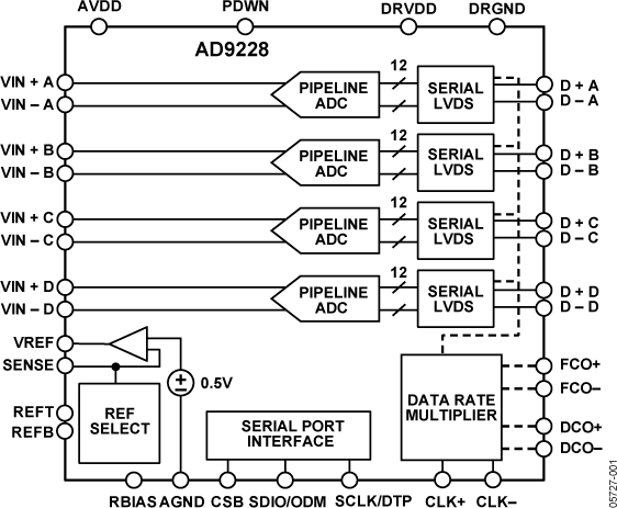
The AD9228 is a quad, 12-bit, 40/65 MSPS analog-to-digital converter (ADC) with an on-chip sample-and-hold circuit designed for low cost, low power, small size, and ease of use. The product operates at a conversion rate of up to 65 MSPS and is optimized for outstanding dynamic performance and low power in applications where a small package size is critical. The ADC requires a single 1.8 V power supply and LVPECL-/ CMOS-/LVDS-compatible sample rate clock for full performance operation. No external reference or driver components are required for many applications. The ADC automatically multiplies the sample rate clock for the appropriate LVDS serial data rate. A data clock output (DCO) for capturing data on the output and a frame clock output (FCO) for signaling a new output byte are provided. Individual channel power-down is supported and typically consumes The ADC contains several features designed to maximize flexibility and minimize system cost, such as programmable clock and data alignment and programmable digital test pattern generation. The available digital test patterns include built-in deterministic and pseudorandom patterns, along with custom user-defined test patterns entered via the serial port interface (SPI). The AD9228 is available in an RoHS compliant, 48-lead LFCSP. It is specified over the industrial temperature range of ?40?C to +85?C.PRODUCT HIGHLIGHTSSmall Footprint. Four ADCs are contained in a small, space-saving package. Low power of 119 mW/channel at 65 MSPS. Ease of Use. A data clock output (DCO) is provided that operates at frequencies of up to 390 MHz and supports double data rate (DDR) operation.User Flexibility. The SPI control offers a wide range of flexible features to meet specific system requirements. Pin-Compatible Family. This includes the AD9287 (8-bit), AD9219 (10-bit), and AD9259 (14-bit).?APPLICATIONSMedical imaging and nondestructive ultrasound Portable ultrasound and digital beam-forming systemsQuadrature radio receivers Diversity radio receivers Tape drives Optical networking Test equipment